Crosswise heterogeneous electron irradiation method of improving global completion table (GCT) chip safe working area

A technology of safe working area and electron irradiation, applied in the manufacturing of circuits, electrical components, semiconductor/solid-state devices, etc., can solve problems such as the improvement bottleneck of the batch safe working area of ​​IGCT devices, reduce the redistribution effect, and improve the overall Safe working area, easy operation effect

Active Publication Date: 2013-04-24
ZHUZHOU CRRC TIMES SEMICON CO LTD
View PDF4 Cites 4 Cited by
  • Summary
  • Abstract
  • Description
  • Claims
  • Application Information

AI Technical Summary

Problems solved by technology

Some practitioners have proposed a scheme to improve the safe working area of ​​IGCT, in which lateral current redistribution and local minority carrier lifetime control technology are two important control technologies, but in fact, due to the differences in actual processes and the non-uniformity between chips The existence of nature makes it a bottleneck to improve the safe working area of ​​actual IGCT devices in batches

Method used


Image

  • Crosswise heterogeneous electron irradiation method of improving global completion table (GCT) chip safe working area
  • Crosswise heterogeneous electron irradiation method of improving global completion table (GCT) chip safe working area
  • Crosswise heterogeneous electron irradiation method of improving global completion table (GCT) chip safe working area

Examples


Embodiment Construction

[0034] The present invention will be further described in detail below in conjunction with the accompanying drawings and specific embodiments.

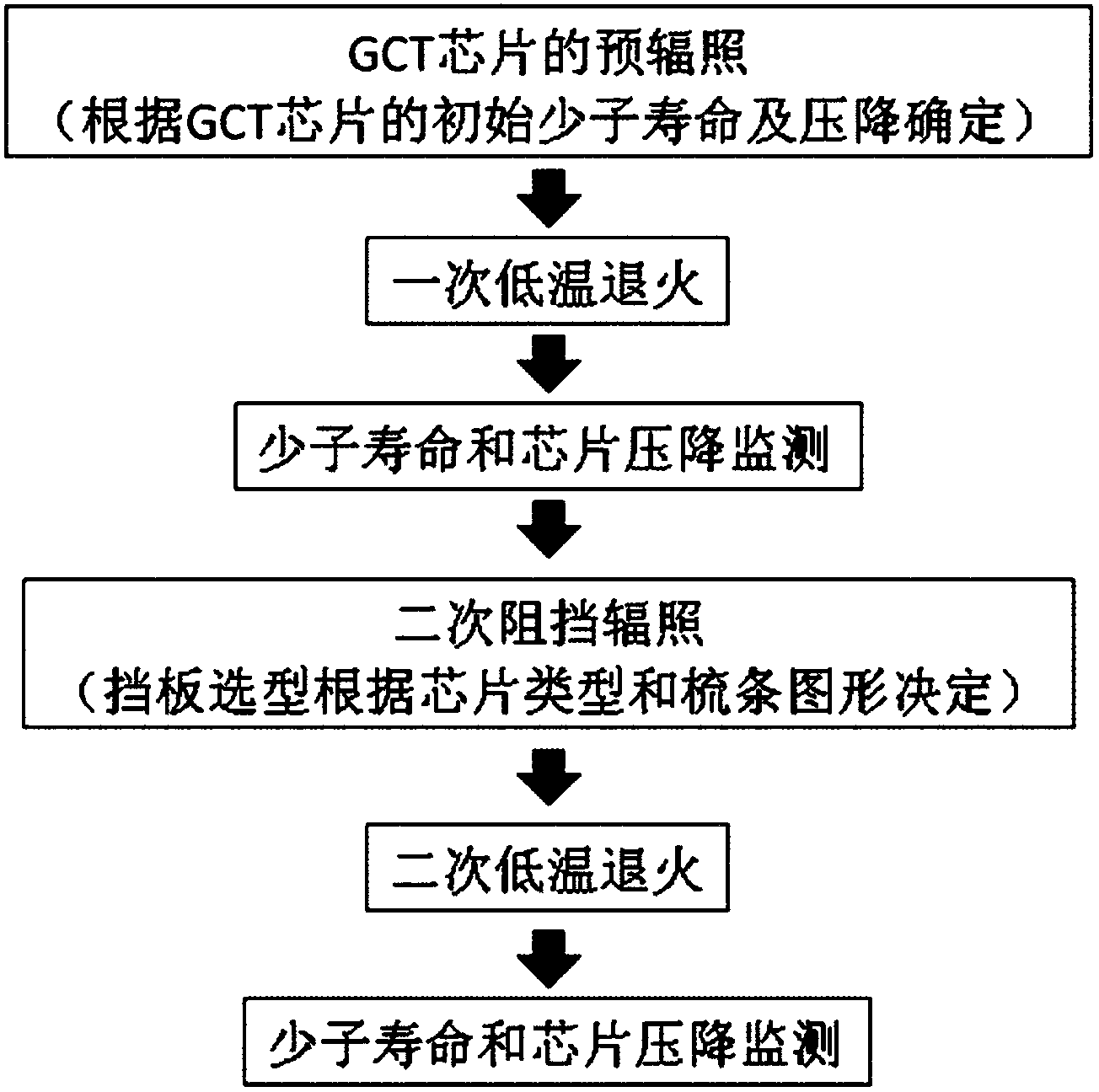
[0035] Such as figure 1As shown, the present invention is a method for improving the lateral non-uniform electron irradiation of the GCT chip safe working area, and its steps are:

[0036] (1) Pre-irradiation of GCT chips. By controlling the minority carrier lifetime and voltage drop of the chip, a pre-irradiation is performed on the GCT chip.

[0037] (2) After primary annealing, monitor the minority carrier lifetime and chip voltage drop.

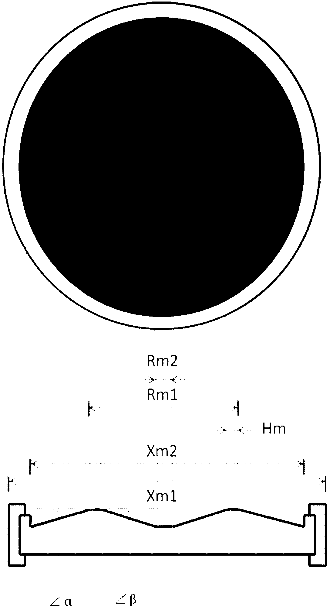
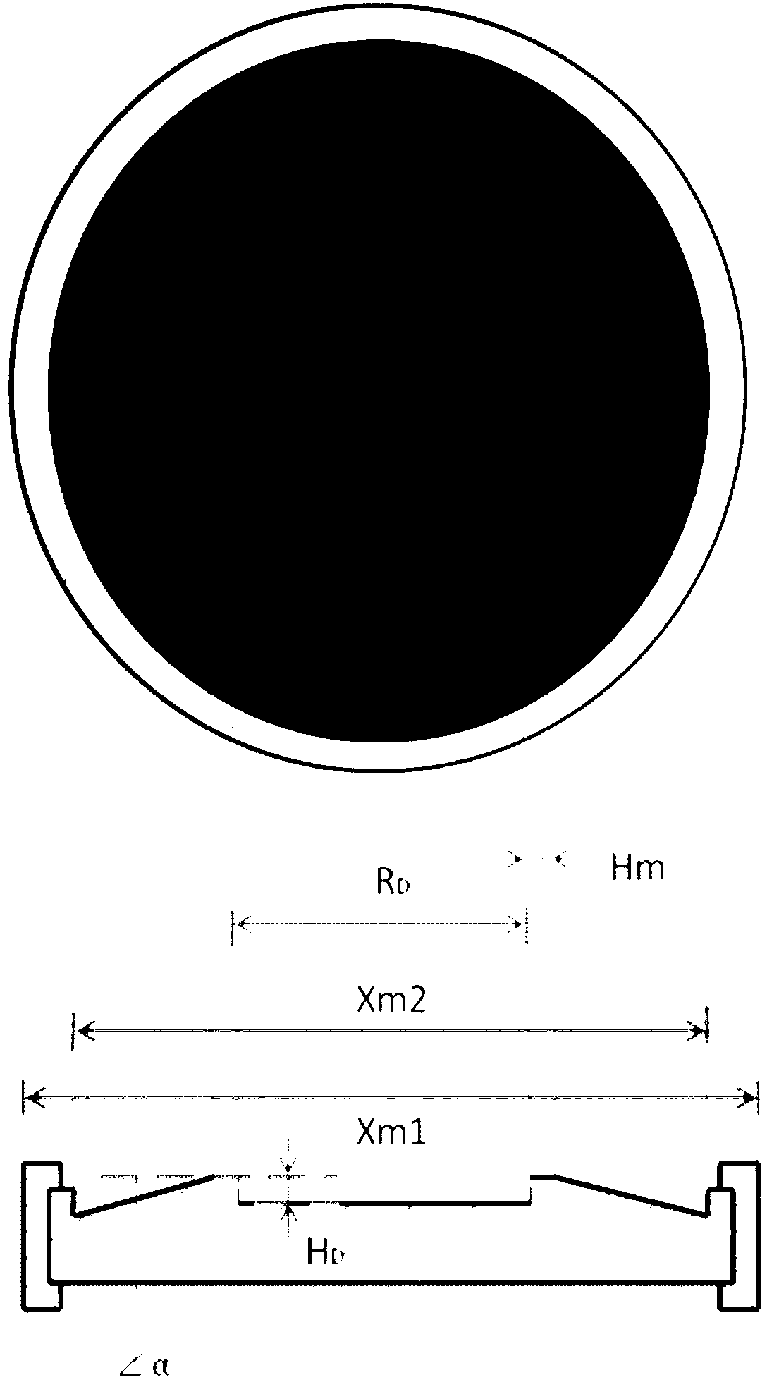
[0038] (3) The composite alloy baffle is used, and the GCT chip is irradiated twice and annealed by using the non-uniformity of the electron irradiation to penetrate the composite alloy baffle, so as to achieve the minority carrier lifetime and pressure drop requirements of the GCT chip. The type of the composite alloy baffle can be determined according to the chip type and the sliver pattern....


PUM


Abstract

Provided is a crosswise heterogeneous electron irradiation method of improving a global completion table (GCT) chip safe working area. The crosswise heterogeneous electron irradiation method of improving the GCT chip safe working area comprises the following steps: (1) carrying out pre-radiation of a GCT chip, and carrying out a primary pre-irradiation to the GCT chip through methods of controlling minority carrier lifetime and pressure drop of the GCT chip, (2) carrying out monitoring of the minority carrier lifetime and pressure drop of the GCT chip after a primary annealing, (3) adopting composite alloy baffles, carrying out a second irradiation and a second annealing to the GCT chip by using heterogeneity of electron irradiation penetrating through the composite alloy baffles, and (4) carrying out the monitoring of the minority carrier lifetime and pressure drop of the GCT chip again. The crosswise heterogeneous electron irradiation method of improving the GCT chip safe working area has the advantages of being simple in principle, and simple and convenient to operate, achieving control of the minority carrier lifetime of parts of the GCT chip, reducing redistribution effect of an electric current in the process of cutoff of GCT by reducing the minority carrier lifetime of far from gate pole slivers, and improving a whole safe working area of the GCT chip and the like.

Description

technical field [0001] The present invention mainly relates to the field of high-power semiconductor devices, in particular to a laterally non-uniform electron irradiation method for improving the safe working area of ​​a GCT chip, and mainly applies to a GCT chip with an independent gate structure and a surrounding discrete comb structure, and at the same time Also suitable for electron irradiation applications of GTO and ETO chips with similar structures. Background technique [0002] High-energy particle irradiation technology is the parameter control technology of high-power semiconductor devices commonly used in the world at present. Its basic principle is to irradiate the semiconductor with a high-energy particle beam with sufficient energy, and the high-energy particle will elastically collide with the lattice atoms in the semiconductor. The lattice atoms are displaced to generate interstitial atom-hole pairs. Corresponding to the generation of these defects, correspo...

Claims


Application Information

Patent Timeline
Patent Type & Authority Applications(China)
IPC IPC(8): H01L21/268
Inventor 刘博冯江华蒋谊张明
Owner ZHUZHOU CRRC TIMES SEMICON CO LTD
Why Eureka
Try Eureka