
Manufacturing method of separated grid type flash memory with peripheral circuit

A manufacturing method and technology of peripheral circuits, which are applied in the fields of circuits, semiconductor/solid-state device manufacturing, electrical components, etc., can solve the problems of polysilicon residue and uneven surface of silicon oxide layer, and achieve the effect of avoiding poor terminal isolation.

Active Publication Date: 2014-09-24
SEMICON MFG INT (SHANGHAI) CORP
View PDF1 Cites 0 Cited by
  • Summary
  • Abstract
  • Description
  • Claims
  • Application Information

AI Technical Summary

Problems solved by technology

Due to the local unevenness caused by shallow trench isolation on the substrate, it will cause the uneven surface of the silicon oxide layer caused by the local height difference, which has always caused the problem of polysilicon residue in the pits on the surface of the silicon oxide layer.

Method used


Image

  • Manufacturing method of separated grid type flash memory with peripheral circuit
  • Manufacturing method of separated grid type flash memory with peripheral circuit
  • Manufacturing method of separated grid type flash memory with peripheral circuit

Examples


Embodiment Construction

[0028] As described in the background technology, during the formation process of the word line gate and the polysilicon layer of the erasable gate on both sides of the separated gate structure, the thickness is difficult to control and cannot meet the ideal requirements, which in turn leads to breakdown between devices The voltage dropped drastically, from the expected 18V, to less than 10V. In view of the problems referred to above, the inventor of the present invention has proposed a kind of word line manufacturing method of the split-gate flash memory with peripheral circuit, and it comprises the following steps:

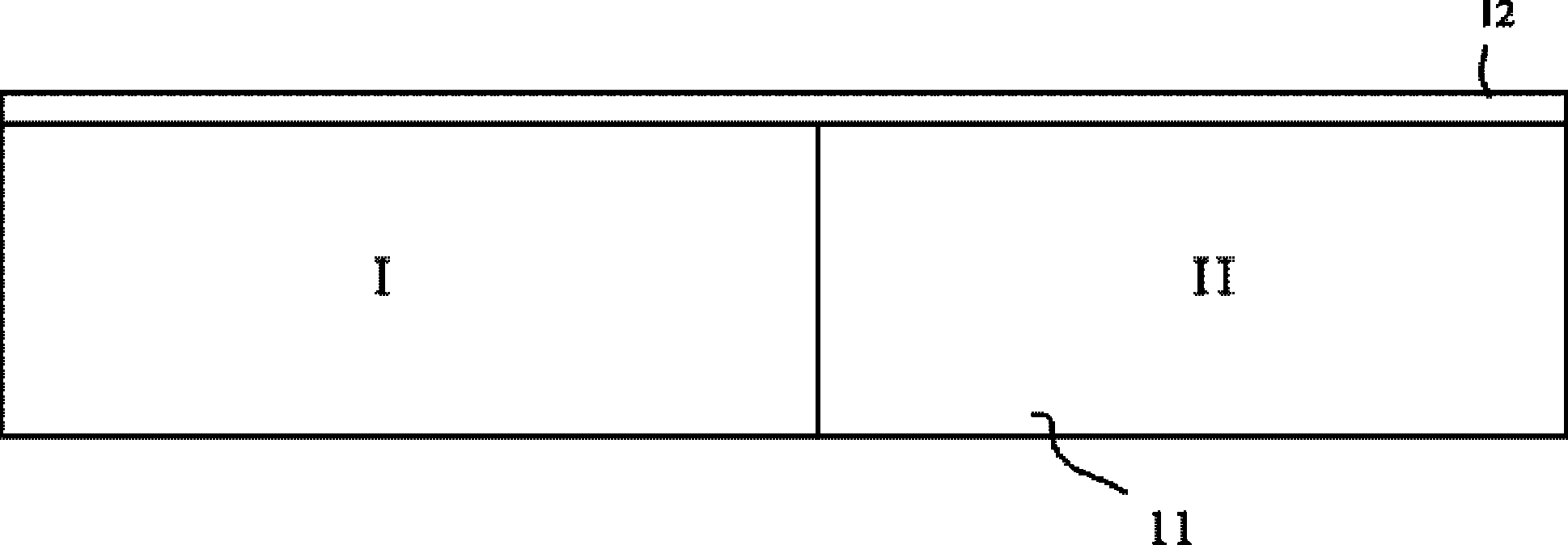
[0029] S1: Provide a semiconductor substrate, the semiconductor substrate includes a first region and a second region, a split-gate flash memory transistor will be subsequently formed on the first region, and a peripheral circuit transistor will be subsequently formed on the second region;

[0030] S2: Form a gate stack in the first region, the gate stack includ...


PUM


Abstract

The invention relates to a manufacturing method of a separated grid type flash memory with a peripheral circuit. The manufacturing method comprises that a semiconductor base provided with a first area and a second area is provided; grid lamination is formed in the first area; a first polycrystalline silicon layer is precipitated, wherein the thickness of the first polycrystalline silicon layer is the needed thickness of a transistor grid of the peripheral circuit; a silicon dioxide layer is formed in the second area; the second silicon dioxide layer is precipitated, at least the surface of the first polycrystalline silicon layer and a concave pit in junction of the first polycrystalline silicon layer and the silicon dioxide layer are filled; the whole is grinded to be smooth in surface in a chemical and mechanical mode; whole etching is conducted until a hard mask film layer is exposed from the first area; and the silicon dioxide layer is removed. According to the manufacturing method of the separated grid type flash memory with the peripheral circuit, the problems that performance of terminal insulation is bad due to chemical and mechanical grinding and residual of polycrystalline silicon caused by local high and low range in a peripheral area are avoided due to organic combination of advantages of chemical and mechanical grinding and terminal detecting of etching, and the circumstance that dielectric layers on lower layer especially a substrate silicon layer are damaged due to over etching of the bottom of the surface concave pit in the process of direct etching is avoided.

Description

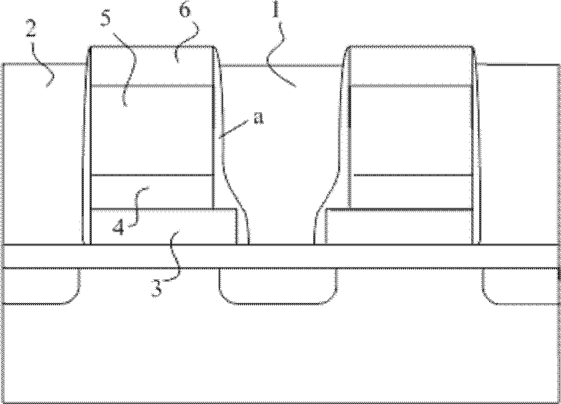
technical field [0001] The invention relates to the technical field of semiconductor manufacturing, in particular to a manufacturing method of a split gate type flash memory with peripheral circuits. Background technique [0002] Random access memory, such as DRAM and SRAM, has the problem of data loss after power failure during use. To overcome this problem, various embedded split-gate flash memories have been designed and developed. At present, the flash memory based on the floating gate concept has become the most common embedded split-gate flash memory due to its small cell size and good working performance. [0003] The gate structure of one of the split-gate flash memory transistors is as follows figure 1 , including a gate stack structure of separated gates, an erasable gate 1 between two adjacent gate stack structures, and word line gates 2 respectively located on two sides of the two gate stack structures away from each other. Wherein, the gate stack structure in...

Claims


Application Information

Patent Timeline
Patent Type & Authority Patents(China)
IPC IPC(8): H01L21/8234
Inventor 王友臻周儒领
Owner SEMICON MFG INT (SHANGHAI) CORP
Learn More