Method for forming fin field effect transistor

A fin field effect and transistor technology, which is applied in semiconductor/solid-state device manufacturing, electrical components, circuits, etc., can solve problems such as difficulty in ensuring stable performance of fin field effect transistors, and achieve uniform distribution of ion implantation

Active Publication Date: 2019-07-30
SEMICON MFG INT (SHANGHAI) CORP +1
View PDF7 Cites 0 Cited by
  • Summary
  • Abstract
  • Description
  • Claims
  • Application Information

AI Technical Summary

Problems solved by technology

[0004] However, as the size of semiconductor devices continues to shrink and the device density increases, the manufacturing process of fin field effect transistors is challenged, and it is difficult to ensure the stable performance of fin field effect transistors

Method used


Image

  • Method for forming fin field effect transistor
  • Method for forming fin field effect transistor
  • Method for forming fin field effect transistor

Examples


Embodiment Construction

[0031] An embodiment of the present invention provides a method for forming a fin field effect transistor, which will be described in detail below with reference to the accompanying drawings.

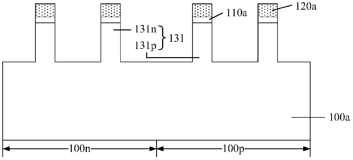
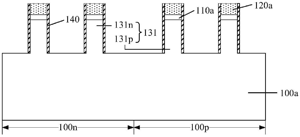
[0032] Figure 1 to Figure 13 It is a schematic cross-sectional view of an intermediate structure of a method for forming a fin field effect transistor according to a specific embodiment of the present invention.

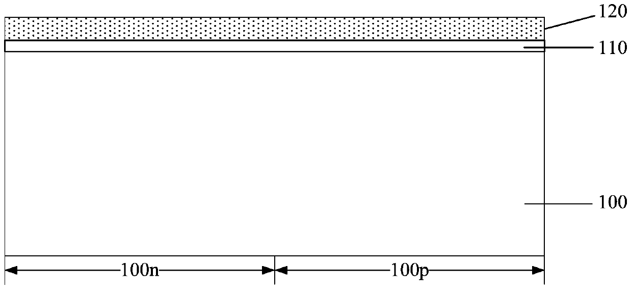
[0033] refer to figure 1 A substrate 100 is provided, and a pad layer 110 and a mask layer 120 are sequentially formed on the surface of the substrate 100 .

[0034] The substrate 100 includes an adjacent NMOS region 100n and a PMOS region 100p. The NMOS region 100n is subsequently used to form an NMOS transistor, and the PMOS region 100p is used to form a PMOS transistor. The substrate 100 is used to provide a platform for subsequent processes, and to form fins by etching.

[0035] In the embodiment of the present invention, the substrate 100 may be a silicon substrate, ...


PUM


Abstract

A method of forming a fin-type field effect transistor comprises the following steps: providing a substrate, wherein multiple fins distributed at intervals are formed on the surface of the substrate, the top of each fin in the multiple fins distributed at intervals forms a first part of a fin, and the part near the substrate forms a second part of the fin; forming a doped layer on the surface of the substrate and on the sidewall surfaces of the second parts of the fins, wherein the doped layer is provided with doped ions inside; carrying out first annealing to make the doped ions in the doped layer diffuse into the second parts of the fins; and forming a deeply doped well in the substrate. According to the embodiment of the invention, as the step of ion implantation into a well region is put after the step of first annealing for driving the doped ions in the doped layer to diffuse into the second parts of the fins, the problem that the ions implanted into the well region diffuse due to first annealing and a poor well region isolation effect is caused is avoided effectively.

Description

technical field [0001] The invention relates to the technical field of semiconductor manufacturing, in particular to a method for forming a fin field effect transistor. Background technique [0002] With the rapid development of semiconductor manufacturing technology, semiconductor devices are developing toward higher component density and higher integration. Transistors, as the most basic semiconductor devices, are currently being widely used. With the improvement of component density and integration of semiconductor devices, the gate size of planar transistors is getting shorter and shorter. The control ability of traditional planar transistors on channel current becomes weaker, resulting in short channel effect and leakage current. affect the electrical performance of semiconductor devices. [0003] In order to overcome the short-channel effect of the transistor and suppress the leakage current, a Fin Field Effect Transistor (Fin FET) is proposed in the prior art. The F...

Claims


Application Information

Patent Timeline
Patent Type & Authority Patents(China)
IPC IPC(8): H01L21/8238H01L21/324
CPCH01L21/324H01L21/823807H01L21/823821
Inventor 周飞
Owner SEMICON MFG INT (SHANGHAI) CORP
Why Eureka
Try Eureka