Array substrate, liquid crystal display and display device

A liquid crystal display, array substrate technology, applied in nonlinear optics, instruments, optics, etc., can solve the problems of not being able to achieve double-sided display and normal viewing, etc.

Active Publication Date: 2016-03-02
BOE TECH GRP CO LTD
View PDF4 Cites 0 Cited by
  • Summary
  • Abstract
  • Description
  • Claims
  • Application Information

AI Technical Summary

Problems solved by technology

In this way, when the transparent display is viewed from the side of the array substrate, it cannot be viewed normally due to the light reflection of the metal signal line, and double-sided display cannot be realized.

Method used


Image

  • Array substrate, liquid crystal display and display device
  • Array substrate, liquid crystal display and display device
  • Array substrate, liquid crystal display and display device

Examples


example 1

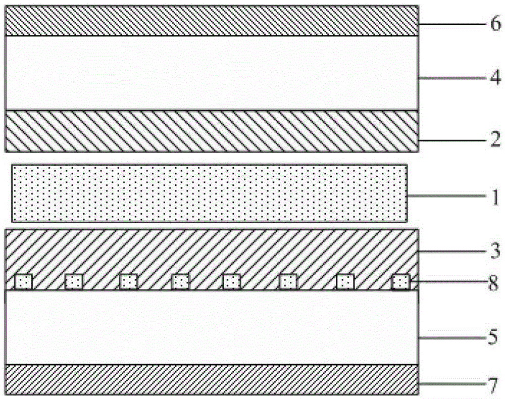
[0039] like Figure 2b As shown, the light blocking layer 04 can be disposed on the side of the base substrate 013 of the array substrate 01 facing the liquid crystal layer 03 , that is, the light blocking layer 04 is disposed between the base substrate 013 and the metal signal line 011 and the TFT device 012 .

example 2

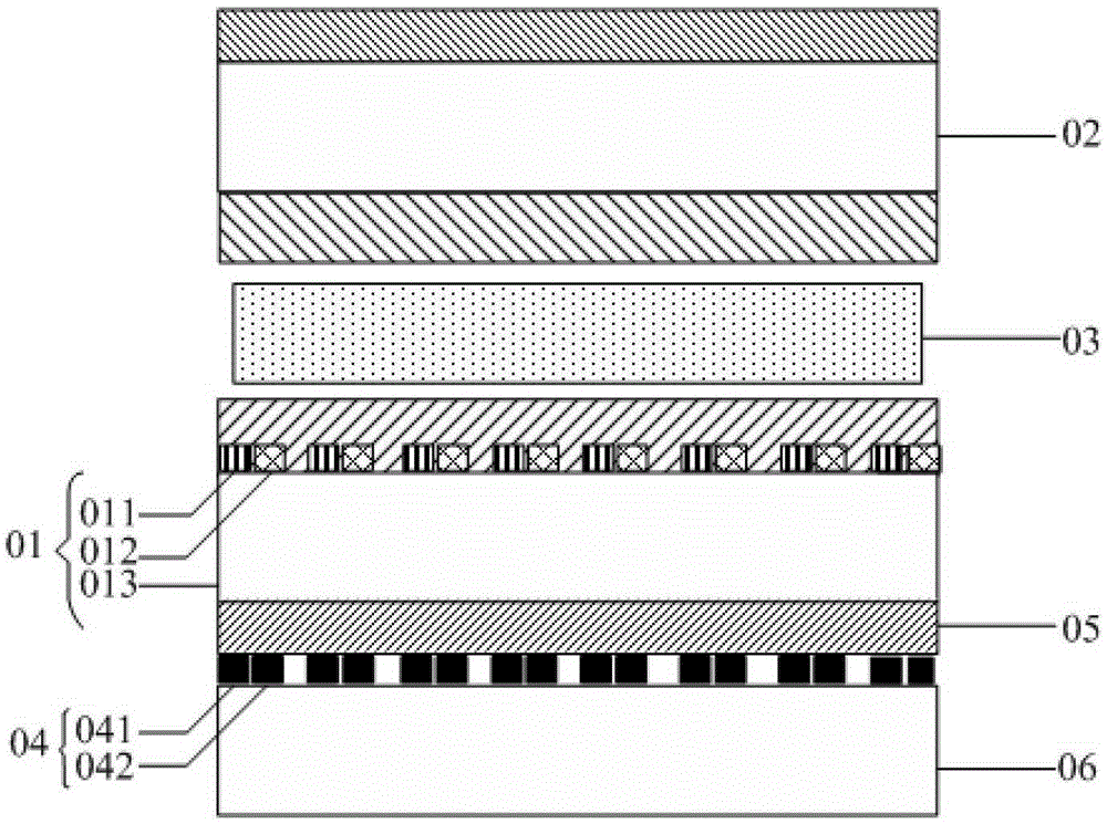
[0041] The light blocking layer 04 may be located on a side of the base substrate 013 of the array substrate 01 away from the liquid crystal layer 03 . Specifically, such as Figure 2c As shown, the light blocking layer 04 may be directly disposed on the side of the base substrate 013 away from the liquid crystal layer 03 .

example 3

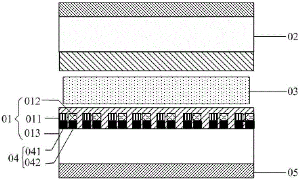
[0043] The light blocking layer 04 may be located on a side of the base substrate 013 of the array substrate 01 away from the liquid crystal layer 03 . Specifically, such as Figure 2d and Figure 2e As shown, a light-shielding substrate 06 may be disposed between the array substrate 01 and the polarizer 05 , and the light-shielding layer 04 may be disposed on the light-shielding substrate 06 . Specifically, such as Figure 2d As shown, the light blocking layer 04 can be arranged on the side of the light blocking substrate 06 facing the array substrate 01; or, as Figure 2e As shown, the light blocking layer 04 may be disposed on the side of the light blocking substrate 06 away from the array substrate 01 . During specific implementation, the light blocking layer 04 may be fabricated on the light blocking substrate 06 first, and then the light blocking substrate 06 is attached to the array substrate 01 .

[0044] Based on the same inventive concept, an embodiment of the pr...


PUM


Abstract

Provided are an array substrate (01), a liquid crystal display screen, and a display device. The liquid crystal display screen comprises the array substrate (01), an opposite-direction substrate (02) opposite to the array substrate (01), and a liquid crystal layer (03) provided between the array substrate (01) and the opposite-direction substrate (02), the array substrate (01) having multiple metal signal lines (011) provided within an effective display area thereof. The liquid crystal display screen further comprises first light shielding portions (041), the first light shielding portions (041) corresponding to the metal signal lines (011) in a one-to-one relationship, and each being located at one side, facing away from the liquid crystal layer (03), of the corresponding metal signal line (011), and an orthographic projection of each first light shielding portion (041) on the array substrate (01) covering an orthographic projection of the corresponding metal signal line (011) on the array substrate (01). Because the disposed first light shielding portion (041) can block the external light from irradiating the metal signal lines (011) from the array substrate (01) side, the metal signal lines (011) are prevented from reflecting the light, thereby improving a viewing effect of a transparent display from the array substrate (01) side and achieving double-side display.

Description

technical field [0001] The invention relates to the technical field of liquid crystal display, in particular to an array substrate, a liquid crystal display and a display device. Background technique [0002] With the continuous development of display technology, transparent displays have emerged. The so-called "transparency" means that the display itself has a certain degree of penetration. As a medium of information, transparent displays can display some product information and related pictures, which greatly improves the attention of products. Favored by the market. [0003] At present, transparent displays are generally made of liquid crystal displays, the main structure of which is as follows: figure 1 As shown, it includes: a liquid crystal layer 1, an upper alignment layer 2, a lower alignment layer 3, a color filter substrate 4, an array substrate 5, an upper polarizer 6, and a lower polarizer 7; wherein, the array substrate 5 is provided with a The gate signal lin...

Claims


Application Information

Patent Timeline
Patent Type & Authority Patents(China)
IPC IPC(8): G02F1/1362G02F1/13
CPCG02F1/133512G02F1/133342G02F1/133567G02F1/13629
Inventor 武延兵
Owner BOE TECH GRP CO LTD
Why Eureka
Try Eureka