ldmos transistor and its manufacturing method

A manufacturing method and transistor technology, which are applied in semiconductor/solid-state device manufacturing, semiconductor devices, electrical components, etc., can solve problems such as reducing device area, and achieve the effect of improving breakdown voltage and high breakdown voltage

Active Publication Date: 2016-12-28
SEMICON MFG INT (SHANGHAI) CORP
View PDF4 Cites 0 Cited by
  • Summary
  • Abstract
  • Description
  • Claims
  • Application Information

AI Technical Summary

Problems solved by technology

For LDMOS, it has become more and more difficult to increase the breakdown voltage of LDMOS as much as possible while reducing the device area.

Method used


Image

  • ldmos transistor and its manufacturing method
  • ldmos transistor and its manufacturing method
  • ldmos transistor and its manufacturing method

Examples


Embodiment Construction

[0030] The LDMOS transistor and its manufacturing method proposed by the present invention will be further described in detail below with reference to the drawings and specific embodiments.

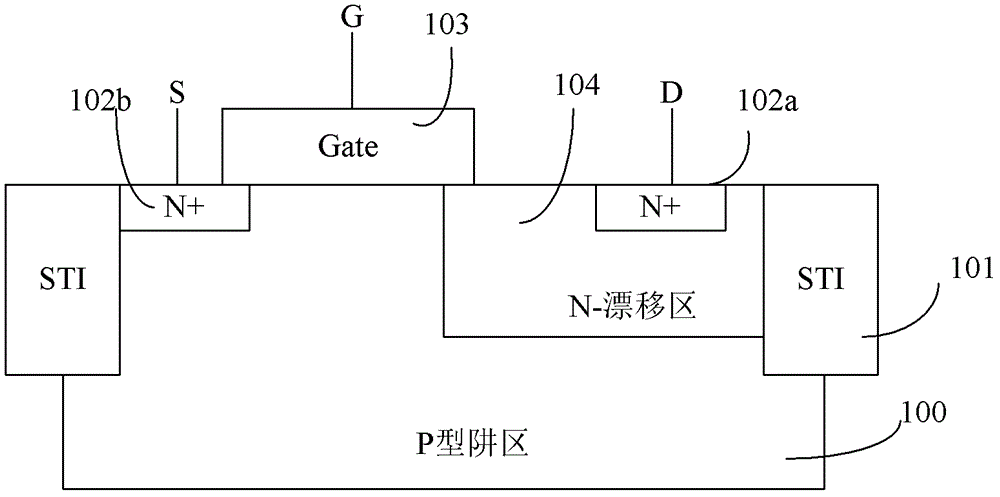
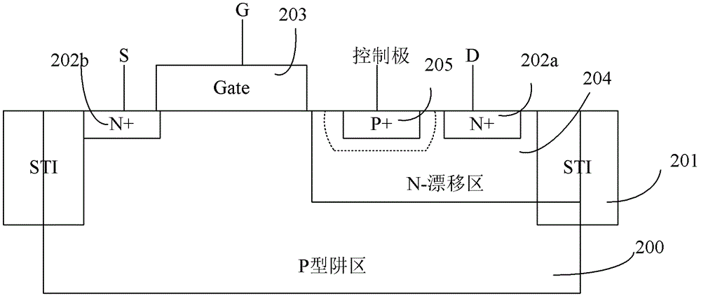
[0031] like figure 2 As shown, the present invention proposes an LDMOS transistor, which includes a semiconductor substrate 200 having a well region, a source region 202b and a drain region located in the surface of the semiconductor substrate 200, and a gate located above the semiconductor substrate 200 ( Gate) 203, wherein the drain region includes a drain drift region 204, a drain contact region 202a located in the drain drift region 204, and a drain tuning region 205 located in the drain drift region 204 and close to the gate 203, The doping type of the drain tuning region 205 is opposite to that of the drain contact region 202a.

[0032] When the well region and the drain tuning region 205 are P-type, the source region 202b, the drain drift region 204 and the drain contact region 2...


PUM


Abstract

The invention provides an LDMOS transistor and a manufacturing method thereof. The LDMOS transistor is enabled to have a structure similar to that of a JFET (junction field effect transistor) through forming a drain electrode tuning region which is inverted with a source and a drain in a drain drift region. The drain tuning region enables the drift region of the LDMOS transistor to become narrow, thereby improving breakdown voltage, and being conducive to manufacturing device chips with higher breakdown voltage and smaller area. The manufacturing method of the LDMOS transistor does not need an additional mask, is capable of forming the drain tuning region while forming a source region and a drain region by heavy doping, and can be completely compatible with the existing CMOS manufacturing process. Meanwhile, the LDMOS transistor can be enabled to have tenability by extracting a control electrode from the drain tuning region.

Description

technical field [0001] The invention relates to the field of semiconductor manufacturing, in particular to an LDMOS transistor and a manufacturing method thereof. Background technique [0002] LDMOS transistor structures are widely used as semiconductor devices for many types of transistor applications such as high voltage MOS field effect transistors. [0003] like figure 1 As shown, a typical LDMOS transistor in the prior art includes: a semiconductor substrate 100 with a P-type well region, an STI (Shallow Trench Isolation Structure) 101 for isolating devices, an N+ doped The source region 102b, the drain region, and the gate structure (Gate) 103 covering the channel region and affecting electron distribution in the channel region. The drain region generally includes a drain contact region 102a and a drain drift region (N-drift region) 104 extending toward the channel region (or gate). Generally, the source S of an LDMOS transistor is drawn from the source region 102 b...

Claims


Application Information

Patent Timeline
Patent Type & Authority Patents(China)
IPC IPC(8): H01L29/78H01L29/06H01L21/336
Inventor 陈乐乐
Owner SEMICON MFG INT (SHANGHAI) CORP
Why Eureka
Try Eureka