Gate driving circuit
A gate drive circuit and stage gate technology, applied in instruments, static indicators, etc., can solve the problems affecting the normal operation of the gate drive circuit, the deterioration of the switching element's turn-off characteristics, and the large leakage current of the switching element. Threshold voltage offset, the effect of reducing the risk of abnormality
- Summary
- Abstract
- Description
- Claims
- Application Information
AI Technical Summary
Problems solved by technology
Method used
Image
Examples
no. 1 example
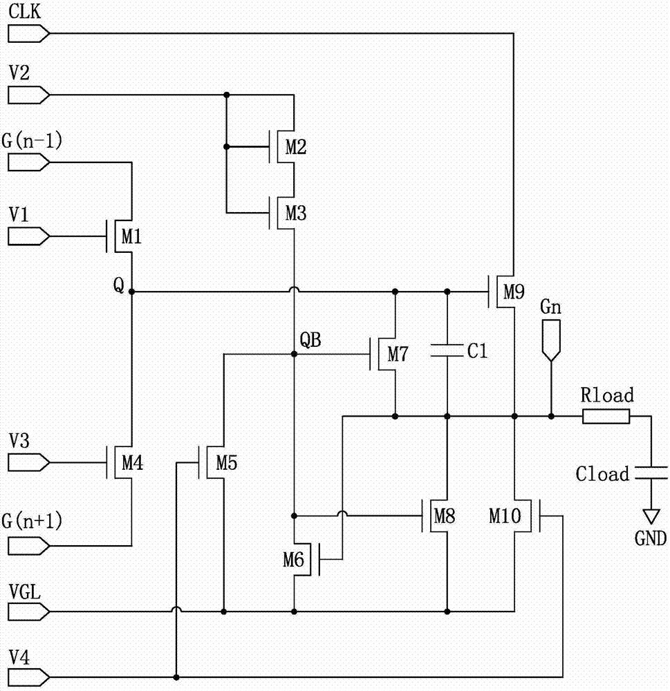
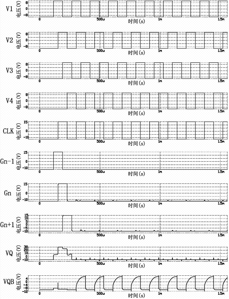
[0037] See figure 2 , which is a timing diagram of the gate driving unit of the first embodiment, as shown in figure 2 As shown, the absolute values of the high level and low level of the first timing signal to the fourth timing signal V1~V4 are equal, and the duty ratios of the first timing signal to the fourth timing signal V1~V4 are all percent Fifty. The first timing signal to the fourth timing signal V1-V4 are sequentially delayed by a quarter cycle, that is to say, the second timing signal V2 is a quarter cycle later than the first timing signal V1, and the third timing signal V3 is later than the first timing signal V1. The second timing signal V2 is a quarter cycle later, and the fourth timing signal V4 is later than the third timing signal V3 by a quarter cycle. The fifth timing signal CLK is synchronized with the second timing signal V2.
[0038] In one embodiment of the present invention, the high level of the first timing signal to the fourth timing signal V...
no. 2 example
[0058] Figure 5 It is a timing schematic diagram of the four-level gate driving unit in the gate driving circuit according to the second embodiment of the present invention. Such as Figure 5 As shown, the high level of the first timing signal to the fourth timing signal V1~V4 is three times the absolute value of the low level, and the duty ratios of the first timing signal to the fourth timing signal V1~V4 are all 100% 25 / 2. That is to say, the product of the amplitude of the high level and the duration of the high level of the first timing signal to the fourth timing signal V1-V4 is equal to the product of the amplitude of the low level and the duration of the low level, so The voltage offsets of the first to fourth switching elements M1-M4, the fiftieth switching element M5, and the tenth switching element M10 when a positive voltage is applied are inverse numbers to the threshold voltage offsets when a negative voltage is applied, Therefore, the left and right offsets ...
PUM
 Abstract
Description
Claims
Application Information


