
Three-dimensional integrated circuits and fabrication thereof

A technology of integrated circuits and manufacturing methods, applied in the directions of circuits, electrical components, electrical solid devices, etc., can solve the problems of loss and occupation of the available area, and achieve the effect of increasing the active area

Inactive Publication Date: 2014-02-12
NAN YA TECH
View PDF8 Cites 1 Cited by
  • Summary
  • Abstract
  • Description
  • Claims
  • Application Information

AI Technical Summary

Problems solved by technology

However, through-substrate vias (TSVs) formed on the active die occupy the available active area, resulting in a loss of available area

Method used


Image

  • Three-dimensional integrated circuits and fabrication thereof
  • Three-dimensional integrated circuits and fabrication thereof
  • Three-dimensional integrated circuits and fabrication thereof

Examples


Embodiment Construction

[0042] Embodiments for practicing the invention are discussed in detail below. It will be appreciated that the embodiments provide many applicable inventive concepts, which can be implemented in wide variation. The specific embodiments discussed are merely intended to invent specific ways of using the embodiments and are not intended to limit the scope of the invention.

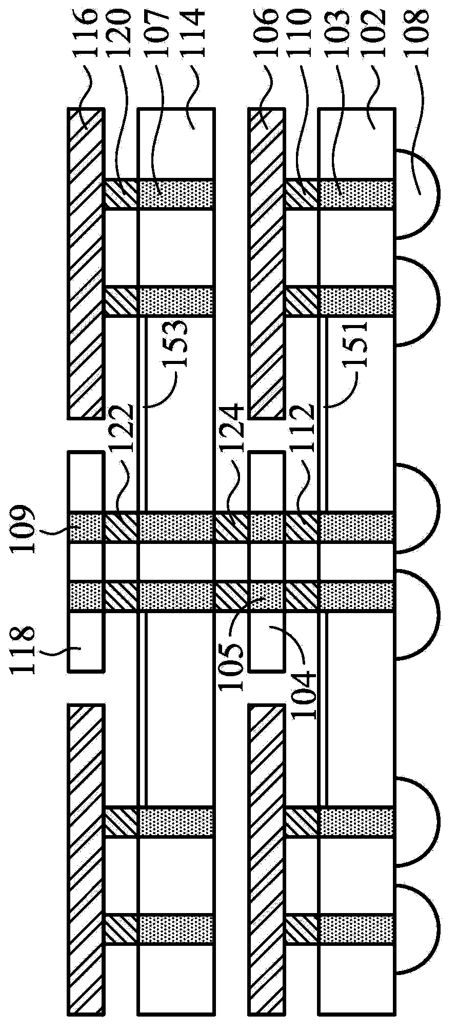
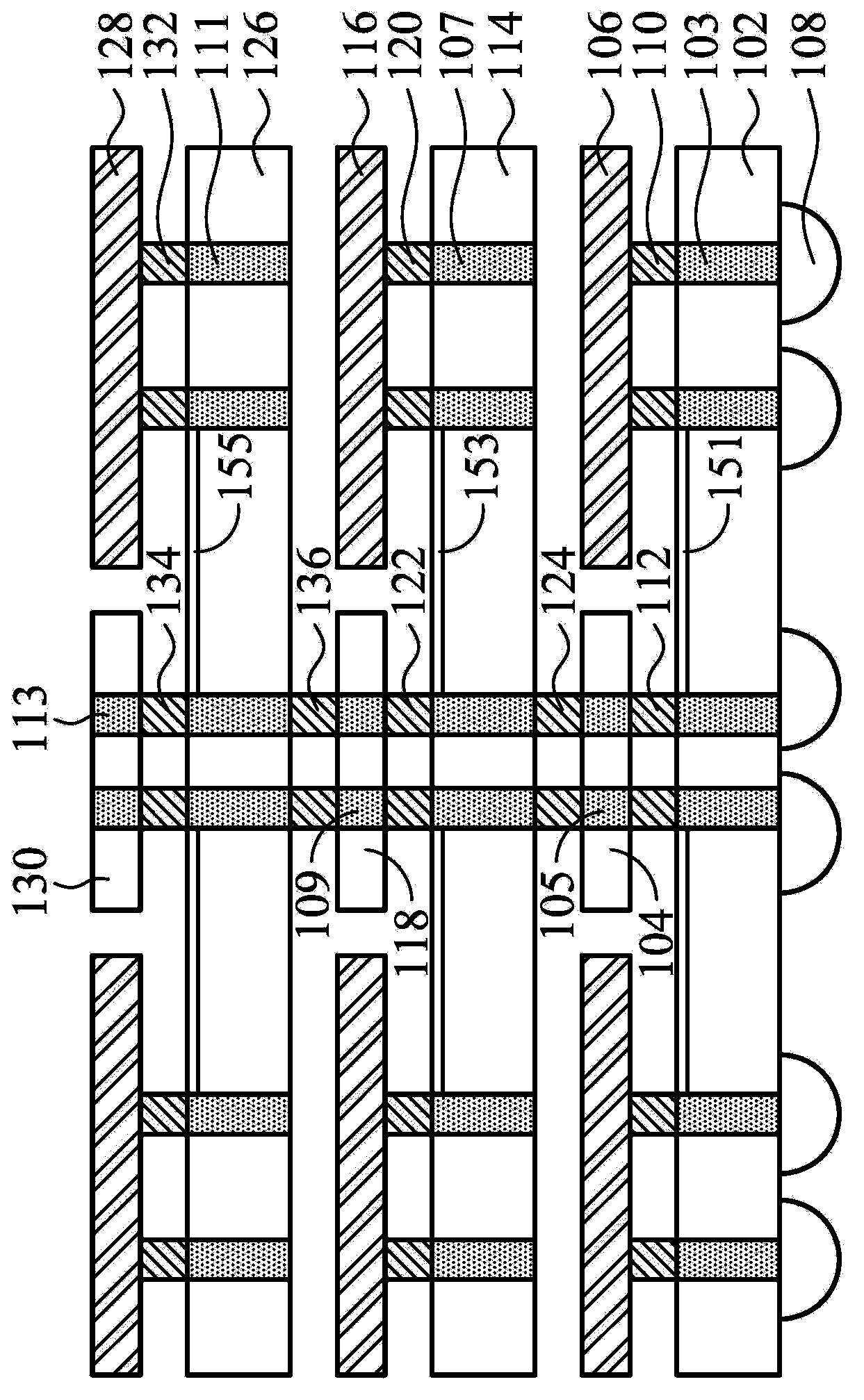
[0043] based on the following Figure 1A~Figure 1D A method for fabricating a three-dimensional integrated circuit (3DIC for short) including an interposer according to an embodiment of the present invention is described. Please refer to Figure 1A , providing a first interposer 102 suitable for integrated circuit manufacturing. The first interposer 102 can be formed of semiconductor materials, such as silicon, silicon germanium, silicon carbide, gallium arsenide or other commonly used semiconductor materials. In another embodiment, the first interposer 102 may be formed of glass, and the first interposer ...


PUM


Abstract

A three-dimensional integrated circuit and fabrication thereof are disclosed, the three-dimensional integrated circuit including a first interposer including through substrate vias (TSV) therein and circuits thereon; a plurality of first active dies disposed on a first side of the first interposer; a plurality of first intermediate interposers, each including through substrate vias (TSV), disposed on the first side of the first interposer; and a second interposer including through substrate vias (TSV) therein and circuits thereon supported by the first intermediate interposers. With the interposers and the intermediate interposers, the three-dimensional integrated circuit can be formed under the condition that no TSVs are formed in the active dies. Therefore, active areas where the active dies are accessible can be increased and the problem of generation of TSV in the active dies can be solved.

Description

technical field [0001] The present invention relates to an integrated circuit, in particular to a three-dimensional integrated circuit (3DIC for short) including an interposer and a manufacturing method thereof. Background technique [0002] Since the invention of the integrated circuit, the semiconductor industry has experienced rapid growth due to continuous improvements in the integration density of various electronic components (eg, transistors, diodes, capacitors, etc.). Generally speaking, the improvement of the above-mentioned integration density comes from the shrinking of the minimum size, so that more components can be integrated on the chip area. [0003] Because the integrated circuit components occupy the surface of the semiconductor wafer, the above described integrated circuit improvements are two-dimensional in nature. Although the improvement of lithography technology can bring considerable improvement to the production of two-dimensional integrated circuit...

Claims


Application Information

Patent Timeline
Patent Type & Authority Applications(China)
IPC IPC(8): H01L25/065H01L23/48H01L21/98H01L21/768
CPCH01L2225/0652H01L2225/06572H01L2924/15331H01L23/49827H01L2224/16235H01L2225/06517H01L2225/06513H01L2225/06541H01L2224/13099H01L24/16H01L25/0652H01L21/768H01L2225/06548H01L23/147H01L2924/00014
Inventor 黄财煜
Owner NAN YA TECH
Learn More