Display panel
A display panel and substrate technology, applied in the direction of electrical components, electric solid devices, circuits, etc., can solve the problem of reducing the light output efficiency of the display panel, and achieve the effect of avoiding reduction and reducing damage
- Summary
- Abstract
- Description
- Claims
- Application Information
AI Technical Summary
Problems solved by technology
Method used
Image
Examples
Embodiment Construction
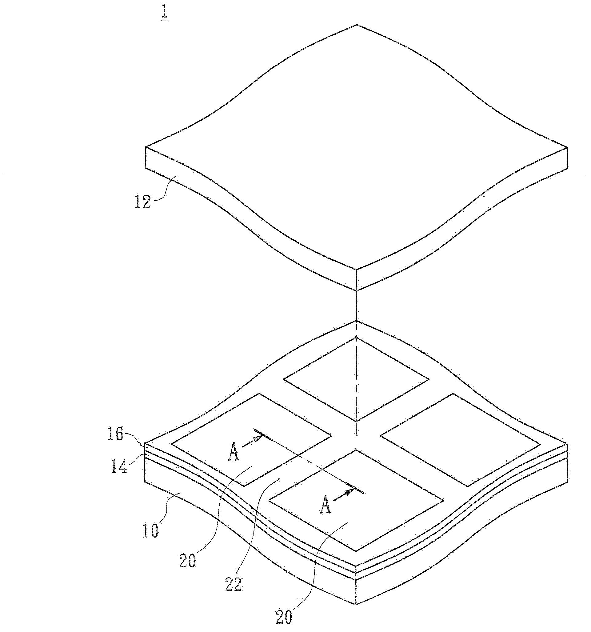
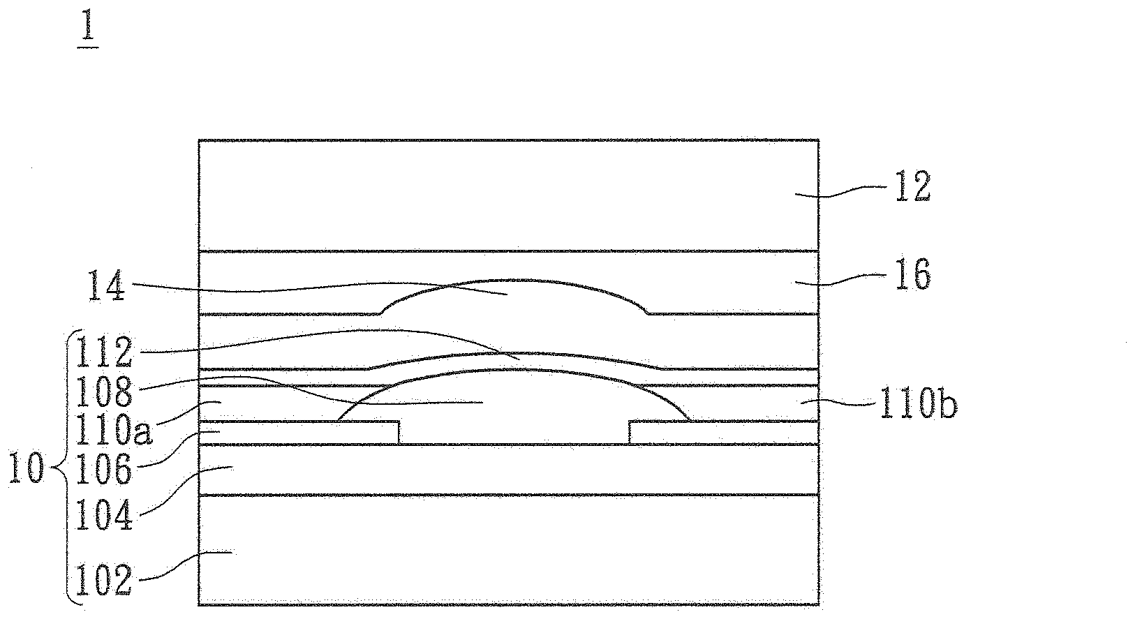
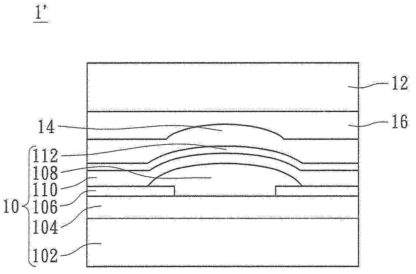
[0040] Please also see figure 1 and Figure 2A , figure 1 A partial perspective view showing a display panel according to an embodiment of the present invention, Figure 2A show evidence figure 1 The schematic cross-sectional view of the display panel along line AA. As shown in the figure, the display panel 1 is a laminated structure formed by sequentially stacking a lower substrate 10 , a sealing film layer 14 , a filling layer 16 and an upper substrate 12 . When viewed from above the display panel 1 (viewed from the side of the upper substrate 12), the upper surface of the lower substrate 10 should have at least one light-emitting region 20 and at least one non-light-emitting region 22, and the non-light-emitting region 22 can be arranged at the Around or between two adjacent light-emitting regions 20 , the present embodiment does not limit the position of the non-light-emitting region 22 on the upper surface of the lower substrate 10 , and those skilled in the art can f...
PUM
 Abstract
Description
Claims
Application Information


