

Multiple quantum well for ultraviolet light emitting diode and a production method therefor
A technology of light-emitting diodes and multiple quantum wells, which is applied to electrical components, circuits, semiconductor devices, etc., can solve the problems of low light-emitting efficiency of light-emitting diodes and achieve the effect of suppressing dislocations
- Summary
- Abstract
- Description
- Claims
- Application Information
AI Technical Summary
Problems solved by technology
Method used
Image

Examples
Embodiment Construction
[0015] Preferred embodiments of the present invention will be described below with reference to the accompanying drawings.
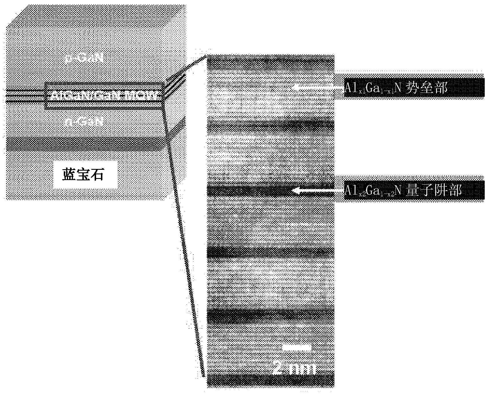
[0016] Such as figure 1 As shown, the ultraviolet light-emitting diode of one embodiment of the present invention uses multiple quantum wells to alternately stack AlN barrier atomic layers and GaN barrier atomic layers on the AlN barrier atomic layers to form Al x1 Ga 1-x1 N barrier section.
[0017] Then, in Al x1 Ga 1-x1 AlN well atomic layers and GaN well atomic layers on the AlN well atomic layers are alternately stacked on the N barrier part to form an Al x2 Ga 1-x2 N quantum well part.
[0018] Here, the Al x1 Ga 1-x1 N barrier and Al x2 Ga 1-x2 In the N quantum well part, use atomic layer deposition (Atomic Layer Deposition; ALD) to perform epitaxy in the crystal growth direction of the reaction substrate by supplying high-voltage aluminum source precursors and gallium source precursors below 400°C. grow.
[0019] On the other hand, Al...
PUM
 Abstract
Description
Claims
Application Information