AlN buffer layer of LED and epitaxial growth method of buffer layer

A technology of epitaxial growth and buffer layer, applied in the direction of electrical components, circuits, semiconductor devices, etc., can solve the problems of large crystal lattice, difficult to grow GaN single crystal film, mismatch and thermal mismatch, etc., to achieve uniform crystal grains, improve Crystal quality and photoelectric properties, effect of dislocation suppression

Active Publication Date: 2018-11-23
XIANGNENG HUALEI OPTOELECTRONICS
View PDF3 Cites 4 Cited by
  • Summary
  • Abstract
  • Description
  • Claims
  • Application Information

AI Technical Summary

Problems solved by technology

However, it is difficult to directly grow high-quality GaN single crystal thin films on heterogen

Method used


Image

  • AlN buffer layer of LED and epitaxial growth method of buffer layer
  • AlN buffer layer of LED and epitaxial growth method of buffer layer
  • AlN buffer layer of LED and epitaxial growth method of buffer layer

Examples


Example Embodiment

[0042] Example 1

[0043] The invention uses magnetron sputtering reaction equipment to prepare an AlN buffer layer on a sapphire substrate, uses metal aluminum (Al) with a purity of 5.5N as the target, and uses helium (Ar) and nitrogen (N 2 ) And oxygen (O 2 ) Is a reactive gas, and the sputtering bias is set to 3000V. Using MOCVD equipment to prepare GaN-based LED epitaxial wafers, using trimethylgallium (TMGa), trimethylindium (TMIn), trimethylaluminum (TMAl) and ammonia (NH3) as sources of Ga, In, Al and N , With silane (SiH 4 ) And Cp2Mg (Cp2Mg) as n-type and p-type doping sources. The specific growth mode is as follows:

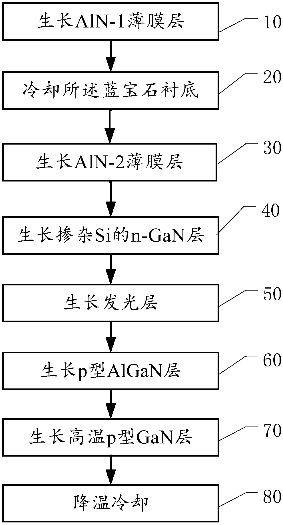
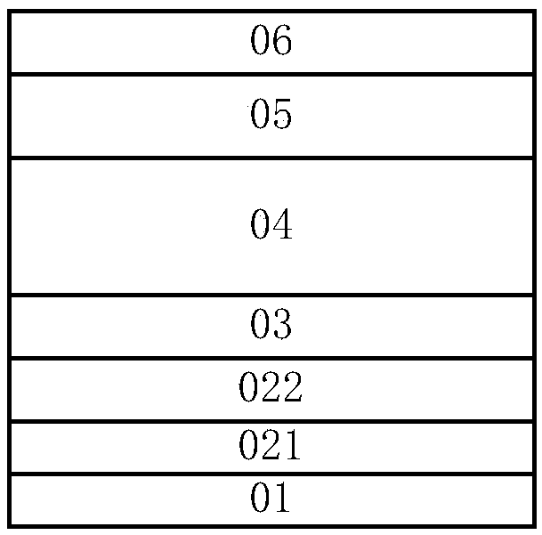
[0044] Please refer to figure 1 with figure 2 , An ALN ​​buffer layer of LED and its epitaxial growth method, including:

[0045] Growing AlN-1 thin film layer, cooling sapphire substrate, growing AlN-2 thin film layer, growing Si-doped n-GaN layer, growing light-emitting layer, growing p-type AlGaN layer, growing high-temperature p-type GaN layer, and cool...

Example Embodiment

[0056] Example 2

[0057] Step 10: Growing AlN-1 thin film layer, specifically:

[0058] Put the sapphire substrate into the magnetron sputtering reaction equipment, heat the sapphire substrate to 650℃, and pass in 30sccm Ar and 120sccm N 2 , And 1sccm O 2 , Control the sputtering bias voltage from 3000V to 2200V, set the target base distance to 3-4cm, and sputter an AlN-1 thin film layer with a thickness of 15-20nm on the surface of the sapphire substrate;

[0059] Step 20: Cooling the sapphire substrate; for example, cooling for 10 minutes.

[0060] Step 30: growing an AlN-2 thin film layer, specifically:

[0061] Put the sapphire substrate with AlN-1 thin film layer into the MOCVD reaction chamber, control the temperature to gradually increase from 850°C to 950°C, keep the reaction chamber pressure at 250mbar, and pass 80L / min of H 2 , 90L / min of NH 3 , 220sccm TMAl source, grow an AlN-2 film with a thickness of 15-20nm on the surface of the AlN-1 film.

[0062] Preferably, the thickn...

Example Embodiment

[0078] Example 3

[0079] The following provides a conventional LED growth method as a comparative example of the present invention.
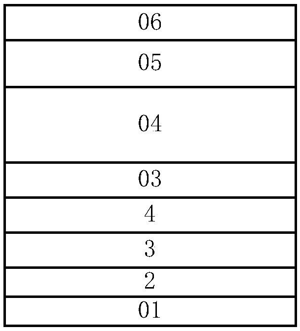
[0080] The conventional LED epitaxial growth method is (see epitaxial layer structure) image 3 ):

[0081] Step 1. Process the sapphire substrate: place the sapphire substrate in the reaction chamber of the metal organic chemical vapor deposition system at a temperature of 900℃-1100℃ 2 In the atmosphere, pass 50L / min-100L / min of H 2 , Keep the reaction chamber pressure 100mbar-200mbar, process the sapphire substrate for 5min-10min.

[0082] Step 2. Grow a GaN low-temperature buffer layer: Cool down to 500°C-600°C, keep the reaction chamber pressure 300mbar-600mbar, and feed NH with a flow rate of 40L / min-60L / min 3 , 50sccm-100sccm TMGa and 50L / min-90L / min H 2 , Growing a GaN low-temperature buffer layer with a thickness of 30nm-60nm on a sapphire substrate.

[0083] Step 3. Grow a 3D GaN layer: increase the temperature to 850°C-1000°C, maintain the rea...


PUM

PropertyMeasurementUnit
Thicknessaaaaaaaaaa

Abstract

The invention discloses an AlN buffer layer of an LED and an epitaxial growth method of the buffer layer. The method comprises the steps of performing growing of an AlN-1 thin film layer, cooling a sapphire substrate, and performing growing of an AlN-2 thin film layer, a Si-doped n-GaN layer, a light-emitting layer, a p-type AlGaN layer and a high-temperature p type GaN layer, and carrying out cooling, wherein the step of performing growing of the AlN-1 thin film layer comprises the steps of putting the sapphire substrate into a magnetron sputtering reaction device to be heated to 650 DEG C, and introducing Ar, N2 and O2, wherein the sputtering bias voltage is controlled to be reduced from 3000V to 2200V, and the target-substrate distance is set to be 3-4cm, and the sputtering thickness ofthe AlN-1 thin film layer is 15-20nm; and the step of performing growing of the AlN-2 thin film layer comprises the steps of putting the sapphire substrate with the AlN-1 thin film layer in an MOCVDreaction cavity, wherein the temperature is controlled to be gradually increased to 950 DEG C from 850 DEG C, the pressure of the reaction chamber is kept to be 250 mbar, and H2, NH3 and a TMAl sourceare pumped, and the AlN-2 thin film layer with the growth thickness of 15-20 nm is grown Compared with the prior art, the brightness of the LED is higher.

Description

technical field [0001] The present invention relates to the technical field of LED epitaxial design application, and more specifically, relates to an ALN ​​buffer layer of LED and an epitaxial growth method thereof. Background technique [0002] At present, LED (Light Emitting Diode, light-emitting diode) is a kind of solid-state lighting. Its advantages such as small size, low power consumption, long service life, high brightness, environmental protection, and durability are recognized by consumers, and the scale of domestic production of LEDs is gradually expanding. ; The demand for LED product performance is increasing day by day in the market. How to grow better epitaxial layers has always been the focus of the LED industry. Because of the improvement of the crystal quality of the epitaxial layer, the performance of LED devices can be improved, and the lifespan and anti-aging ability of LEDs , antistatic ability, and stability will increase with the improvement of the cr...

Claims


Application Information

Patent Timeline
IPC IPC(8): H01L33/12H01L33/00
CPCH01L33/007H01L33/12
Inventor 徐平
Owner XIANGNENG HUALEI OPTOELECTRONICS
Why Eureka
Try Eureka