Semiconductor device

a semiconductor laser and active layer technology, applied in the direction of semiconductor lasers, lasers, solid-state devices, etc., can solve the problems of reducing the yield of the nitride semiconductor laser device, reducing the absorption power of al, ga, and reducing the luminous efficiency, so as to suppress the dislocation of the active layer, suppress the deterioration of the device characteristic, and suppress the effect of dislocation

Active Publication Date: 2009-04-14
EPISTAR CORP
View PDF29 Cites 4 Cited by
  • Summary
  • Abstract
  • Description
  • Claims
  • Application Information

AI Technical Summary

Benefits of technology

[0012]As mentioned above, according to the semiconductor device of the first aspect, the nitride semiconductor layer is formed on the surface of the semiconductor substrate formed of at least two kinds of group III elements and nitrogen. The nitride semiconductor layer is formed of the same constituent elements of the semiconductor substrate. The composition ratio of the lightest element among the group III elements of the constituent elements is higher than the composition ratio of the corresponding element of the semiconductor substrate. That is the composition ratio of the lightest element having a high bonding strength to nitrogen is increased. Accordingly, when the semiconductor device layer is grown on the nitride semiconductor layer, it is possible to easily bond the nitrogen, which is the constitute element of a semiconductor device layer, to the lightest element among the group III elements in the constituent elements of the nitride semiconductor layer. This makes it possible to suppress occurrence of pit in the semiconductor layer which forms the semiconductor device and formed on the nitride semiconductor layer. Therefore, it is possible to suppress deterioration in device characteristic of the semiconductor device. Furthermore, the composition ratio of the lightest element of the nitride semiconductor layer formed on the surface of the semiconductor substrate is higher than the semiconductor substrate. With this composition ratio, the nitride semiconductor layer gets harder than the semiconductor substrate. This makes it possible to bend dislocation which exists in the semiconductor substrate, at the boundary surface between the semiconductor substrate and the nitride semiconductor layer. Thereby, it is possible to suppress dislocation, which exists in the semiconductor substrate, propagated over the nitride semiconductor layer to the semiconductor device layer of higher layer. Also, the dislocation of the semiconductor device layer can be reduced as compared with the conventional case. This also makes it possible to suppress deterioration in device characteristic of the semiconductor device. Furthermore, the semiconductor substrate is formed of at least two kinds of group III elements and nitrogen, it is possible to reduce the lattice constant difference between the semiconductor substrate and the cladding layer, when the semiconductor substrate has the same constituent element of a cladding layer formed on the semiconductor substrate. Accordingly, it is possible to suppress occurrence of a warp and a crack in the semiconductor substrate, which derive from the lattice constant difference between the semiconductor substrate and the cladding layer.
[0024]In the semiconductor device according to the second aspect of the present invention, the nitride semiconductor layer is preferably formed in such a way to come into contact with an upper surface of the semiconductor layer being at the side of the active layer side. According to this structure, dislocation which exists in the semiconductor layer can be bent by the nitride semiconductor layer formed on the surface of the active layer of the semiconductor layer. As a result, it is possible to effectively suppress dislocation from being propagated to the semiconductor device layers formed on the nitride semiconductor device.

Problems solved by technology

However, the conventional nitride semiconductor laser device described in Japanese Unexamined Application No. 2000-140052 has the following drawback.
This disadvantageously causes a reduction in yield of the nitride semiconductor laser device.
A decrease, however, in absorption power of Al, Ga, and N which are constituent elements of the nitride semiconductor layer growing on the AlGaN substrate leads to a drawback.
This tends to create pit and dislocation in the light-emitting device grown on the AlGaN substrate, causing a problem of a deteriorated device characteristic of the semiconductor device.
This disadvantageously causes a reduction in luminous efficiency due to the strain in the active layer (luminous layer).
As a result, this also causes a problem of a deteriorated device characteristic.

Method used


Image

  • Semiconductor device
  • Semiconductor device
  • Semiconductor device

Examples


first embodiment

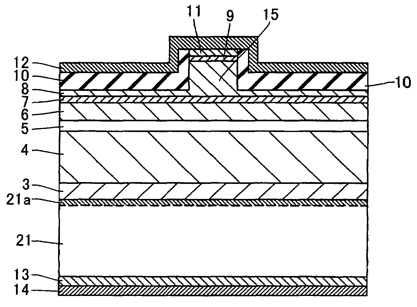
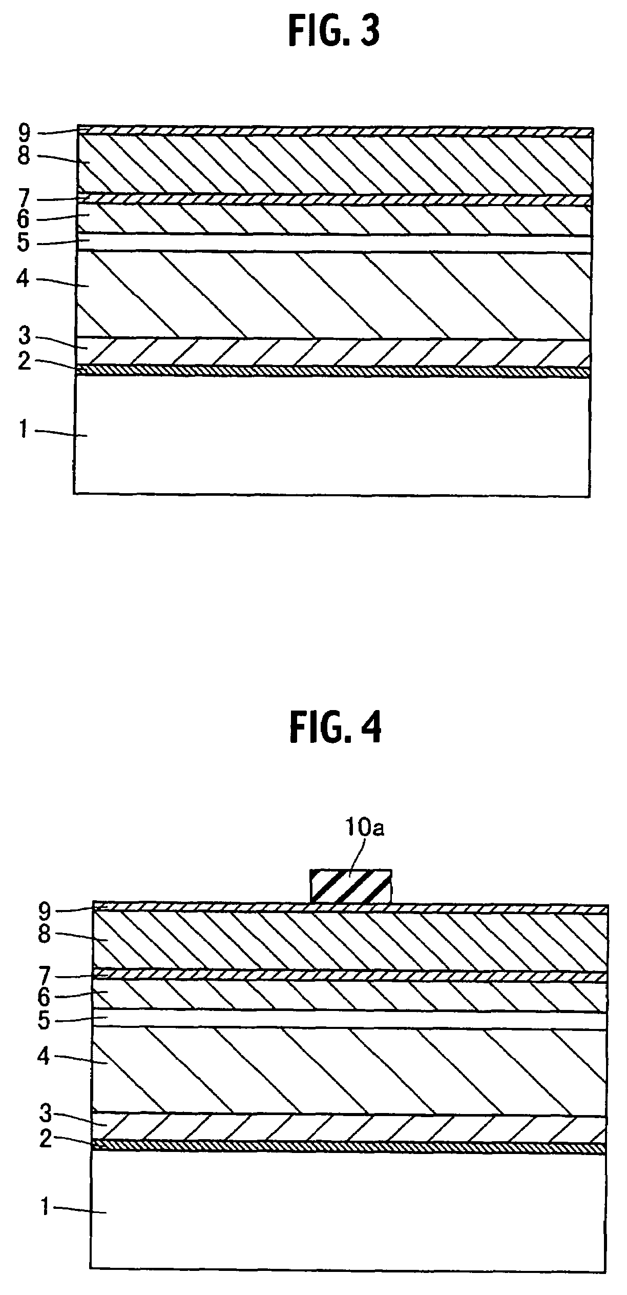
[0055]FIG. 1 is a cross-sectional view illustrating a structure of a nitride semiconductor laser device (semiconductor device) according to a first embodiment of the present invention. FIG. 2 is a cross-sectional view illustrating a structure of an active layer of the nitride semiconductor laser device according to the first embodiment illustrated in FIG. 1. First, an explanation will be given of the structure of the nitride semiconductor laser device according to the first embodiment with reference to FIGS. 1 and 2.

[0056]In the nitride semiconductor laser device according to the first embodiment, as illustrated in FIG. 1, on an AlGaN substrate 1, made of Al0.07Ga0.93N with a thickness of about 100 μm, there is formed a high Al composition layer 2 made of undoped Al0.15Ga0.85N with a thickness of about 0.5 nm to 20 nm. The high Al composition layer 2 is an example of the “nitride semiconductor layer” of the present invention. Also, the AlGaN substrate 1 is an example of the “semicon...

second embodiment

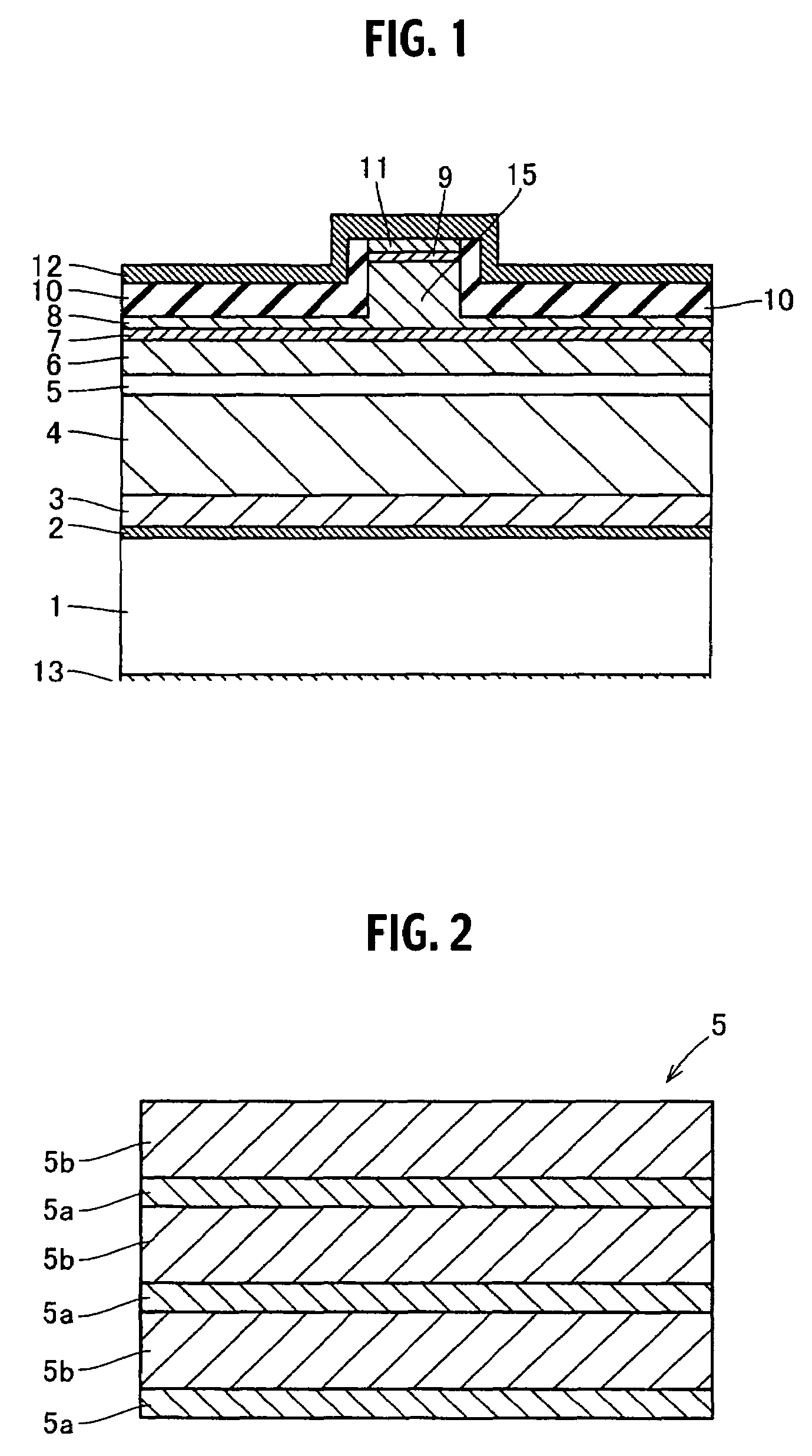
[0077]FIG. 7 is a cross-sectional view illustrating a structure of a nitride semiconductor laser device according to a second embodiment of the present invention. With reference to FIG. 7, in the second embodiment, explanations will be given of a structure of the nitride semiconductor laser device of a case where a high Al composition layer 21a is formed of an altered layer made by alternating a surface of the AlGaN substrate 21, which is not like the first embodiment. In addition, the rest of the structure, other than the AlGaN substrate 21 and the Al composition layer 21a, of the second embodiment is the same as that of the first embodiment. Therefore, only the high composition layer 21a will be explained, and the explanation of the rest of the structure will be omitted. It should be noted that the AlGaN substrate 21 is an example of the “semiconductor substrate” of the present invention.

[0078]In the second embodiment, as illustrated in FIG. 7, the high Al composition layer 21a is...

third embodiment

[0088]FIG. 8 is a cross-sectional view illustrating a structure of a nitride semiconductor laser device (semiconductor device) according to a third embodiment of the present invention. With reference to FIG. 8, in the third embodiment, explanations will be given of a structure of a nitride semiconductor laser device of a case where a high Ga composition layer 31a is formed, on an InGaN substrate 31, as an altered layer, which is not like the first and the second embodiments.

[0089]In the nitride semiconductor laser device according to the third embodiment, as illustrated in FIG. 8, the high Ga composition layer 31a is formed on the InGaN substrate 31 made of In0.15Ga0.85N with a thickness of about 100 μm to about 200 μm. It should be noted that the high Ga composition layer 31a is an example of the “nitride semiconductor layer” of the present invention, and that the InGaN substrate 31 is an example of “semiconductor substrate.”

[0090]In the third embodiment here, the high Ga compositi...


PUM


Abstract

A semiconductor device includes a semiconductor substrate formed of at least two kinds of group III elements and nitrogen, an active layer formed on the semiconductor substrate, and a nitride semiconductor layer formed on a surface of the semiconductor substrate and formed between the semiconductor substrate and the active layer. The nitride semiconductor layer is formed of the same constituent elements of the semiconductor substrate. A composition ratio of the lightest element among the group III elements of the nitride semiconductor layer is higher than a composition ratio of the corresponding element of the semiconductor substrate.

Description

CROSS REFERENCE TO RELATED APPLICATIONS[0001]This application is based upon and claims the benefit of priority from prior Japanese Patent Application No. 2005-263264, filed on Sep. 12, 2005; the entire contents of which are incorporated herein by reference.BACKGROUND OF THE INVENTION[0002]1. Field of the Invention[0003]The present invention relates to a semiconductor device, and more particularly to a semiconductor device having a nitride semiconductor layer.[0004]2. Description of the Related Art[0005]In recent years, the use of nitride semiconductor devices as light sources for large capacity optical disc has been expected and the development has become active. Moreover, conventionally, there are known nitride semiconductor laser devices in which a nitride semiconductor layer is formed on a GaN substrate as a nitride semiconductor substrate (see, for example, Japanese Unexamined Application No. 2000-140052).[0006]Japanese Unexamined Application No. 2000-140052 discloses a structur...

Claims


Application Information

Patent Timeline
Patent Type & Authority Patents(United States)
IPC IPC(8): H01L21/00H01L33/06H01L33/20H01L33/32H01L33/40
CPCB82Y20/00H01L33/32H01S5/34333H01L33/0075H01L33/12H01S5/0217H01S5/2009H01S5/2214H01S5/2231H01S2301/173H01S2304/04H01S2304/12
Inventor KANO, TAKASHIHATA, MASAYUKINOMURA, YASUHIKO
Owner EPISTAR CORP
Why Eureka
Try Eureka