Method for protecting layer by forming hydrocarbon-based extremely thin film

a technology of hydrocarbon-based films and protective layers, applied in semiconductor devices, semiconductor/solid-state device details, electrical devices, etc., can solve the problems of reducing the size of semiconductor devices, increasing the demand for further thinning of these films, and more difficult to obtain films with sufficient chemical resistance and barrier properties, so as to improve the chemical resistance of the covered layer, improve the adhesion of the dopant thin film, and increase the concentration of dopant elements

Active Publication Date: 2018-02-20
ASM IP HLDG BV
View PDF1378 Cites 326 Cited by
  • Summary
  • Abstract
  • Description
  • Claims
  • Application Information

AI Technical Summary

Benefits of technology

[0008]Some embodiments provide a method for protecting a layer, comprising: (i) providing a substrate having a target layer; and (ii) forming a protective layer on the target layer, said protective layer contacting and covering the target layer and containing a hydrocarbon-based layer constituting at least an upper part of the protective layer, which hydrocarbon-based layer is formed by plasma-enhanced atomic layer deposition (PEALD) using an alkylaminosilane precursor and a noble gas without a reactant. In some embodiments, the target layer is a doped layer which may be a dopant thin film formed by SSD processes. In some embodiments, the protective layer is a cap layer which replaces a conventional cap layer in its entirety. In some embodiments, the protective layer is an additional cap layer formed on top of a conventional cap layer. In some embodiments, the protective layer can effectively block dispersion of dopant elements dissociated from the dopant thin film during storage and during a subsequent annealing process so as to increase the concentration of dopant elements in an underlying layer, e.g., a silicon substrate, on which the dopant thin film is formed, while improving chemical resistance of the layer covered by the protective layer. In some embodiments, the protective layer can also be deposited before depositing a dopant thin film for suppressing oxidation of an underlying layer and improving adhesion of the dopant thin film with the underlying layer. In some embodiments, the protective layer can be applied to a layer other than a dopant thin film, where, for example, the protective layer is formed on an underlying layer, e.g., a silicon substrate, before depositing a silicon oxide film or titanium oxide film, for example, on the underlying layer for suppressing oxidation of the underlying layer and improving adhesion with the underlying layer.

Problems solved by technology

However, as the size of semiconductor devices has been reduced, further thinning of these films is in demand.
Also, since lowering the process temperature is in demand, it becomes more difficult to obtain films having sufficient chemical resistance and barrier properties.
However, the increase of thickness of the dopant thin film or the increase of thickness of the cap film may interfere with the standard fabrication processes.

Method used


Image

  • Method for protecting layer by forming hydrocarbon-based extremely thin film
  • Method for protecting layer by forming hydrocarbon-based extremely thin film
  • Method for protecting layer by forming hydrocarbon-based extremely thin film

Examples


example 1

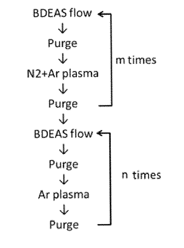
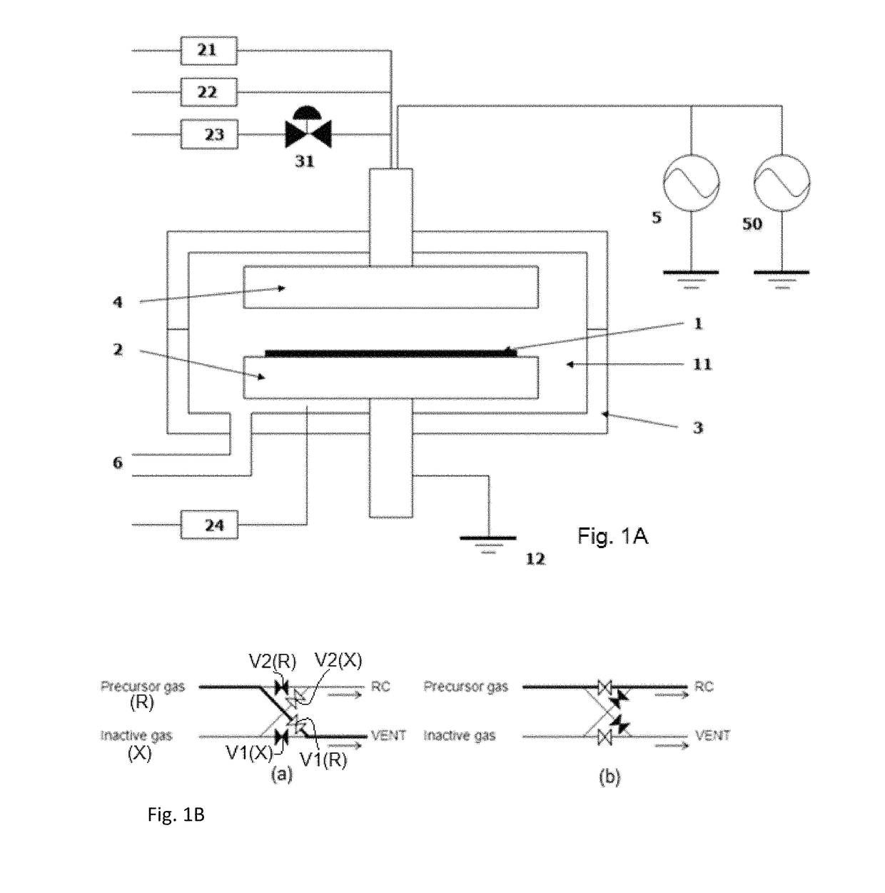
[0074]In this example, a hydrocarbon-based layer (H-cap layer) was deposited on a SiN film formed on a Si substrate (Φ300 mm) by PEALD using the PEALD apparatus illustrated in FIG. 1A (including a modification illustrated in FIG. 1B) with the sequence illustrated in FIG. 6 which corresponds generally to the sequence illustrated in FIG. 7. As illustrated in FIG. 6, by repeating m times a step of feeding an aminosilane precursor (bisdiethylaminosilane (BDEAS)) and a step of applying a N2+Ar plasma alternately under the conditions shown in Table 5, a SiN film having a thickness of 1.5 to 6 nm was deposited. Thereafter, continuously, by repeating n times (30 times) a step of feeding the aminosilane material and a step of applying an Ar plasma alternately under the conditions shown in Table 6, an H-cap layer having a thickness of about 0.1 nm was deposited on the SiN film.

[0075]

TABLE 5(the numbers are approximate)Conditions forSiN filmPrecursor pulse (sec): Supply time3.0SecSubstrate tem...

example 2

[0081]In this example, a SiO2 film which had high moisture absorbency was deposited using TEOS on a substrate, and then annealed at a temperature of 400° C. to dehydrate the film. Thereafter, a SiN film having a thickness of 1.5 nm was deposited on the SiO2 film, followed by deposition of an H-cap layer in a manner which was substantially the same as in Example 1. Changes in film stress of the resultant film with time were measured immediately after completion of the deposition processes. As comparative examples, no SiN film was deposited on the SiO2 film (Comparative Example 3), a SiN film having a thickness of 1.5 nm was deposited in the same manner as in Example 2 without forming an H-cap layer (Comparative Example 4), and a SiN film having a thickness of 2.5 nm was deposited in the same manner as in Example 2 without forming an H-cap layer (Comparative Example 5). The results are shown in FIG. 10. FIG. 10 is a graph showing film stress of layers according to Example 2 (“⋄ SiN 1....

examples 3 and 4

[0083]In this example, a hydrocarbon-based layer (H-cap layer) was deposited on a BSG or PSG film formed on a Si substrate (Φ300 mm) by PEALD using the PEALD apparatus illustrated in FIG. 1A (including a modification illustrated in FIG. 1B) with the sequence illustrated in FIG. 8 under conditions shown in Table 8 below. A SiO cap film was deposited in a manner substantially similar to that for depositing the H-cap film, except that a reactant gas (O2) was fed to the reaction chamber.

[0084]

TABLE 8B / PSG filmAminoSiB / PSiO capH-capFeedFeed + RFfilmfilmDepo rateSiO [times]10NANAB / P [times]010Bottle Temp[° C.]35.035.050.035.0BTL Ar[sccn]2,0002,0002,0002,000O2 / DCM[sccm]1,0001,0001,0000Ar / DCM[sccm]1,0001,0001,0001,000Seal He / DCM[sccm]200200200200RC Press[Pa]400400400400HRF[W]NA200800500SUS Temp[° C.]300300300300SHD Temp[° C.]150150150150Wal Temp[° C.]130130130130Gap[mm]7.57.57.57.5Shift time [sec]Source Feed0.30.30.30.3Source Purge0.90.80.40.4RF-ON00.40.20.2Post Purge00.10.10.1Cycle time1.2...


PUM

PropertyMeasurementUnit
thicknessaaaaaaaaaa
thicknessaaaaaaaaaa
thicknessaaaaaaaaaa

Abstract

A method for protecting a layer includes: providing a substrate having a target layer and forming a protective layer on the target layer, said protective layer contacting and covering the target layer and containing a hydrocarbon-based layer constituting at least an upper part of the protective layer, which hydrocarbon-based layer is formed by plasma-enhanced atomic layer deposition (PEALD) using an alkylaminosilane precursor and a noble gas without a reactant.

Description

BACKGROUND OF THE INVENTION[0001]Field of the Invention[0002]The present invention relates generally to a method for protecting a layer, including a method for capping a doped layer to block diffusion of dopants, by forming a hydrocarbon-based extremely thin film by plasma-enhanced atomic layer deposition (PEALD).[0003]Related Art[0004]A SiN film can be formed by plasma-enhanced atomic layer deposition (PEALD) at a temperature of 400° C. or less without causing chemical or physical damage to an underlying layer, and thus, application of the film as an impurity-dispersion blocking film, a pore-seal film for low-k dielectric film, and a protective film for next-generation memory devices has been studied. However, as the size of semiconductor devices has been reduced, further thinning of these films is in demand. Also, since lowering the process temperature is in demand, it becomes more difficult to obtain films having sufficient chemical resistance and barrier properties.[0005]For exa...

Claims


Application Information

Patent Timeline
Patent Type & Authority Patents(United States)
IPC IPC(8): H01L23/31H01L21/02H01L21/324
CPCH01L23/3192H01L21/324H01L21/02274H01L21/0228H01L21/56H01L21/02167H01L21/02115H01L21/02118
Inventor KATO, RICHIKAOKURO, SEIJINAMBA, KUNITOSHINONAKA, YUYANAKANO, AKINORI
Owner ASM IP HLDG BV
Why Eureka
Try Eureka