Method for protecting layer by forming hydrocarbon-based extremely thin film
a technology of hydrocarbon-based films and protective layers, applied in semiconductor devices, semiconductor/solid-state device details, electrical devices, etc., can solve the problems of reducing the size of semiconductor devices, increasing the demand for further thinning of these films, and more difficult to obtain films with sufficient chemical resistance and barrier properties, so as to improve the chemical resistance of the covered layer, improve the adhesion of the dopant thin film, and increase the concentration of dopant elements
- Summary
- Abstract
- Description
- Claims
- Application Information
AI Technical Summary
Benefits of technology
Problems solved by technology
Method used
Image
Examples
example 1
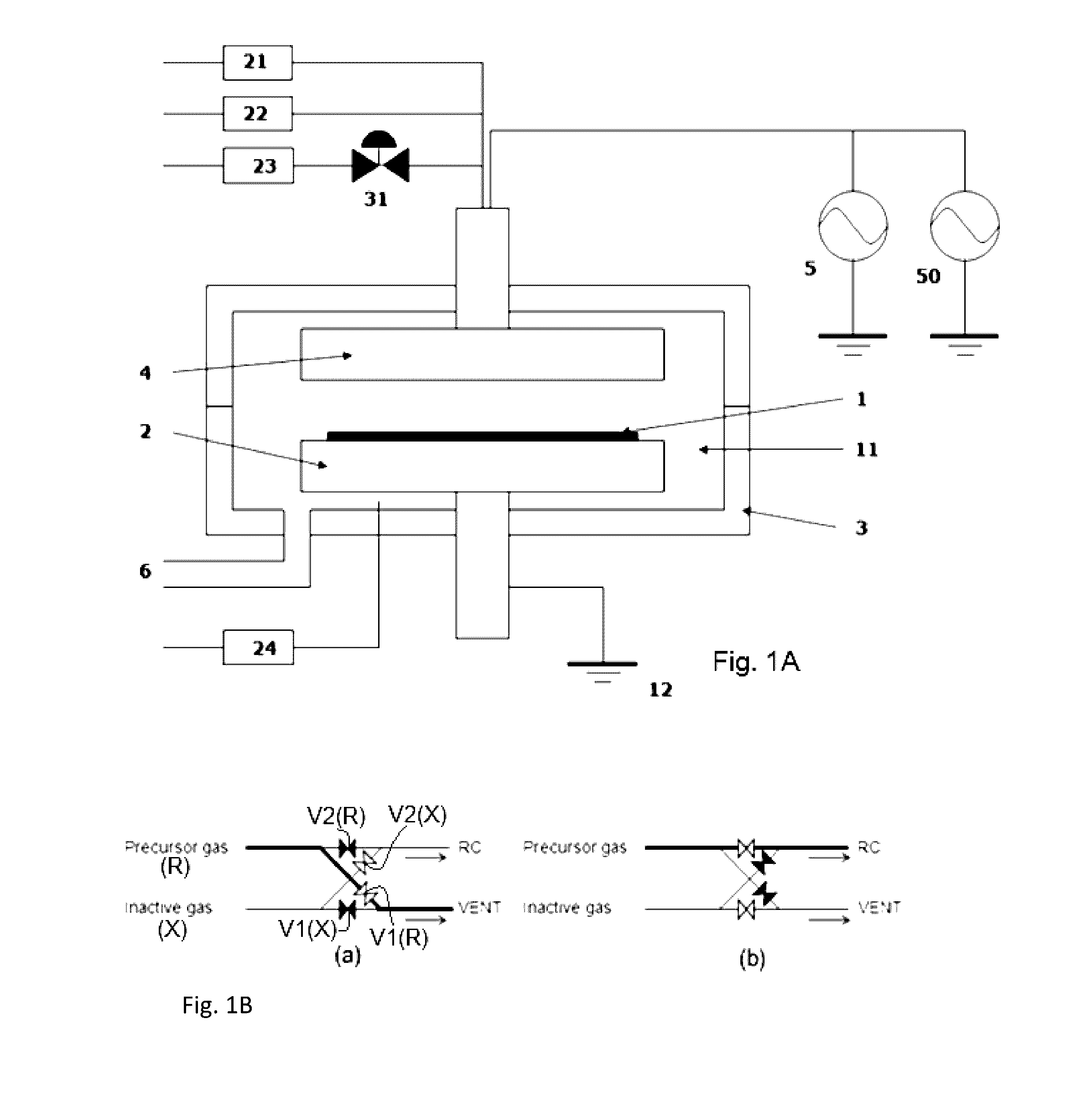
[0071]In this example, a hydrocarbon-based layer (H-cap layer) was deposited on a SiN film formed on a Si substrate (Φ300 mm) by PEALD using the PEALD apparatus illustrated in FIG. 1A (including a modification illustrated in FIG. 1B) with the sequence illustrated in FIG. 6 which corresponds generally to the sequence illustrated in FIG. 7. As illustrated in FIG. 6, by repeating m times a step of feeding an aminosilane precursor (bisdiethylaminosilane (BDEAS)) and a step of applying a N2+Ar plasma alternately under the conditions shown in Table 5, a SiN film having a thickness of 1.5 to 6 nm was deposited. Thereafter, continuously, by repeating n times (30 times) a step of feeding the aminosilane material and a step of applying an Ar plasma alternately under the conditions shown in Table 6, an H-cap layer having a thickness of about 0.1 nm was deposited on the SiN film.
TABLE 5(the numbers are approximate)Conditions forSiN filmPrecursor pulse (sec): Supply time3.0SecSubstrate temperatu...
example 2
[0075]In this example, a SiO2 film which had high moisture absorbency was deposited using TEOS on a substrate, and then annealed at a temperature of 400° C. to dehydrate the film. Thereafter, a SiN film having a thickness of 1.5 nm was deposited on the SiO2 film, followed by deposition of an H-cap layer in a manner which was substantially the same as in Example 1. Changes in film stress of the resultant film with time were measured immediately after completion of the deposition processes. As comparative examples, no SiN film was deposited on the SiO2 film (Comparative Example 3), a SiN film having a thickness of 1.5 nm was deposited in the same manner as in Example 2 without forming an H-cap layer (Comparative Example 4), and a SiN film having a thickness of 2.5 nm was deposited in the same manner as in Example 2 without forming an H-cap layer (Comparative Example 5). The results are shown in FIG. 10. FIG. 10 is a graph showing film stress of layers according to Example 2 (“⋄ SiN 1....
examples 3 and 4
[0077]In this example, a hydrocarbon-based layer (H-cap layer) was deposited on a BSG or PSG film formed on a Si substrate (Φ300 mm) by PEALD using the PEALD apparatus illustrated in FIG. 1A (including a modification illustrated in FIG. 1B) with the sequence illustrated in FIG. 8 under conditions shown in Table 8 below. A SiO cap film was deposited in a manner substantially similar to that for depositing the H-cap film, except that a reactant gas (O2) was fed to the reaction chamber.
TABLE 8B / PSG filmAminoSiB / PSiO capH-capFeedFeed + RFfilmfilmDepo rateSiO [times]10NANAB / P [times]010Bottle Temp[° C.]35.035.050.035.0BTL Ar[sccn]2,0002,0002,0002,000O2 / DCM[sccm]1,0001,0001,0000Ar / DCM[sccm]1,0001,0001,0001,000Seal He / DCM[sccm]200200200200RC Press[Pa]400400400400HRF[W]NA200800500SUS Temp[° C.]300300300300SHD Temp[° C.]150150150150Wal Temp[° C.]130130130130Gap[mm]7.57.57.57.5Shift time [sec]Source Feed0.30.30.30.3Source Purge0.90.80.40.4RF-ON00.40.20.2Post Purge00.10.10.1Cycle time1.21.61.0...
PUM
| Property | Measurement | Unit |
|---|---|---|
| thickness | aaaaa | aaaaa |
| thickness | aaaaa | aaaaa |
| thickness | aaaaa | aaaaa |
Abstract
Description
Claims
Application Information


