Method and apparatus for manufacturing semiconductor substrate dedicated to semiconductor device, and method and apparatus for manufacturing semiconductor device

a semiconductor substrate and manufacturing method technology, applied in the direction of laser beam welding apparatus, manufacturing tools, welding/soldering/cutting articles, etc., can solve the problems of hardly obtaining sufficient gettering capability, and unable to meet the requirements of high-performance semiconductor devices. , to achieve the effect of suppressing the generation and extension of crystal dislocation, facilitating the formation of gettering sink, and reducing the generation of crystal dis

Active Publication Date: 2013-01-22
SUMCO CORP
View PDF18 Cites 4 Cited by
  • Summary
  • Abstract
  • Description
  • Claims
  • Application Information

AI Technical Summary

Benefits of technology

[0068]In a method for manufacturing the semiconductor substrate dedicated to a semiconductor device according to first to third aspects of the present invention, since a multi-photon absorption process is generated in the micro-region inside the semiconductor substrate by condensing laser beams into any micro-region inside the semiconductor substrate, it is possible to readily form the gettering sink by changing only the crystal structure of the corresponding micro-region.
[0069]Particularly, according to the first aspect of the present invention, in the process of forming the gettering sink, the gettering sink is formed in any 3-dimensional shape broadening in parallel with the one surface of the semiconductor substrate and extending in a thickness direction of the semiconductor substrate. Therefore, it is possible to form the gettering sink having little dislocation defect by suppressing generation and extending of a crystal dislocation caused by condensing the laser beam.
[0070]In the method for manufacturing a semiconductor device according to a first aspect of the present invention, it is possible to readily manufacture a high performance semiconductor device, in which heavy metals are reliably trapped, with in a short time.
[0071]In the method for manufacturing a semiconductor substrate dedicated to a semiconductor device according to a second aspect of the present invention, during the substrate heating process, the semiconductor substrate is heated in a predetermined temperature range, for example, greater than or equal to 400° C. and less than or equal to 1000° C. Therefore, it is possible to suppress an excessive temperature change caused by the condensed laser beam so as to prevent a temperature of the semiconductor substrate from locally rapidly rising or falling.
[0072]In the vicinity of the condensing spot of the laser beam, the temperature of the single crystal silicon instantaneously rises to a high temperature. Therefore, if the laser beam is incident to the semiconductor substrate, for example, at a room temperature, a thermal shock wave is generated in the vicinity of the condensing spot, and an internal stress is locally generated. Such an internal stress is alleviated by a thermal process such as a subsequent device formation process, and a dislocation expands from the gettering sink that has been provided, so that a device characteristic may be degraded.
[0073]As described in the second aspect of the present invention, when the semiconductor substrate is previously heated through the substrate heating process in a predetermined temperature range, for example, greater than or equal to 400° C. and less than or equal to 1000° C., it is possible to reduce a temperature difference between a highest temperature in the vicinity of the condensing spot and the temperature of the entire semiconductor substrate when the laser beam is incident. Therefore, it is possible to prevent an excessive temperature change caused by forming the gettering site using a laser beam and suppress generation of an internal stress. In addition, it is possible to form a semiconductor substrate dedicated to a semiconductor device having little possibility of generating the dislocation defect.

Problems solved by technology

If impurities such as heavy metals are introduced into the silicon substrate, a device characteristic is remarkably degraded due to a generation of a leak current or the like.
However, most of the heat treatments performed after forming the device on the silicon substrate are performed at a temperature less than or equal to 400° C., and the heavy metals introduced in the thinning process after forming the device may not be sufficiently trapped.
In the thinning process of a silicon substrate having such a thickness level, since most of the gettering sinks formed on the silicon substrate are removed by grinding, a sufficient gettering capability is hardly obtained.
Therefore, in the EG method in which the gettering site such as backside defect is formed on the back surface of the silicon wafer, it may be difficult to form the gettering sink on the back surface.

Method used


Image

  • Method and apparatus for manufacturing semiconductor substrate dedicated to semiconductor device, and method and apparatus for manufacturing semiconductor device
  • Method and apparatus for manufacturing semiconductor substrate dedicated to semiconductor device, and method and apparatus for manufacturing semiconductor device
  • Method and apparatus for manufacturing semiconductor substrate dedicated to semiconductor device, and method and apparatus for manufacturing semiconductor device

Examples


second embodiment

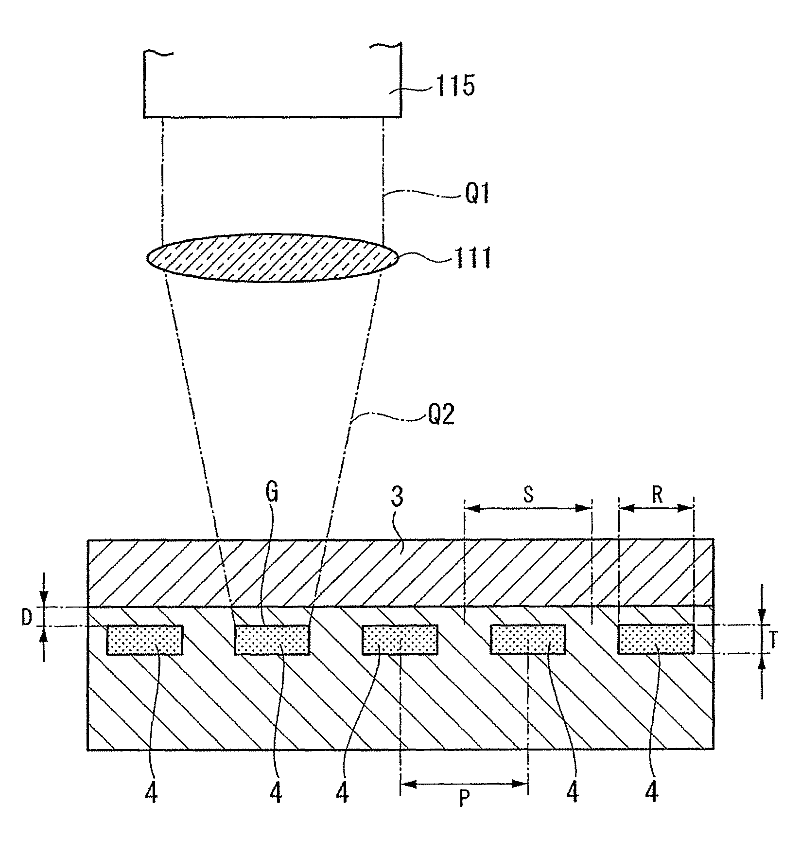
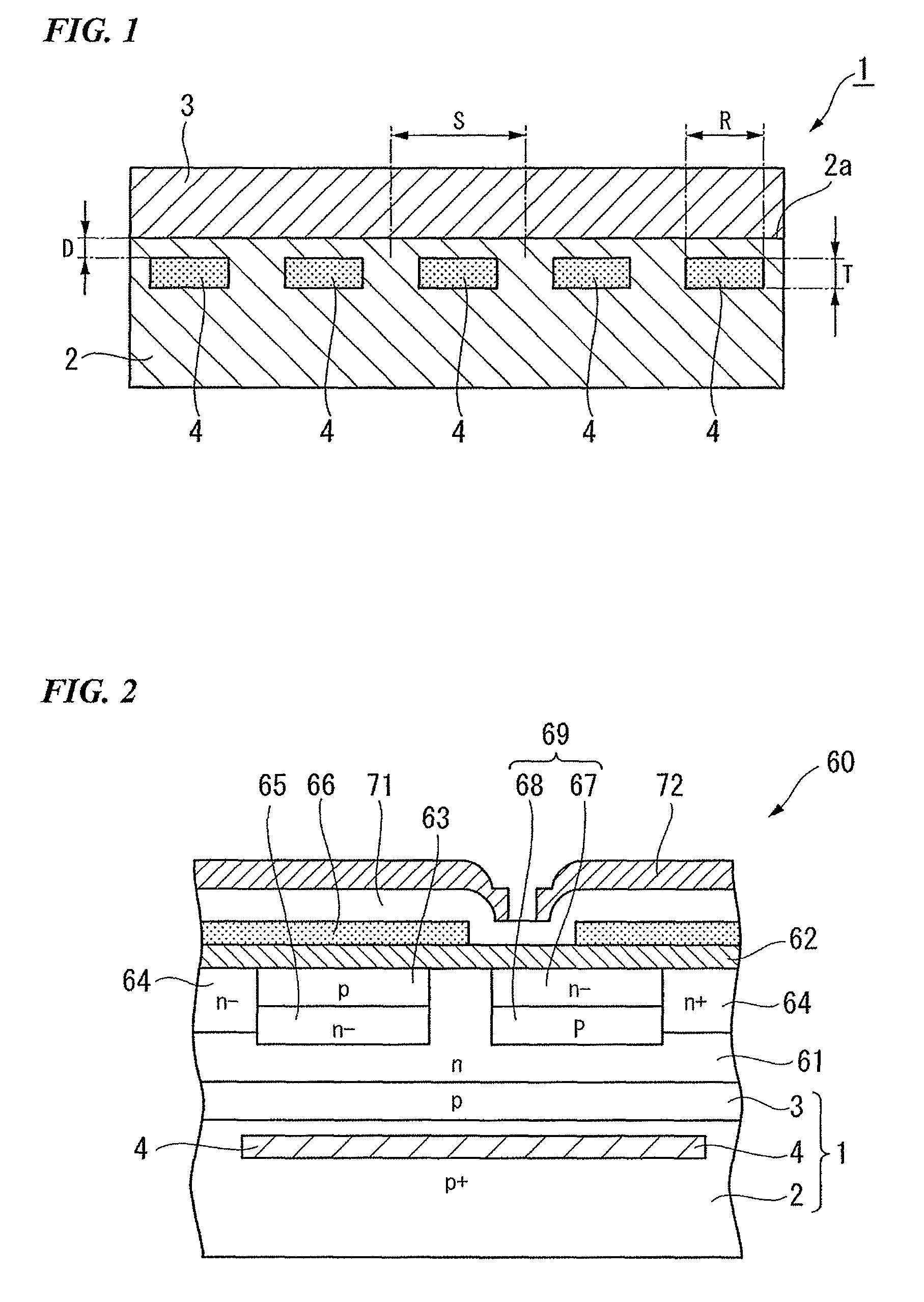
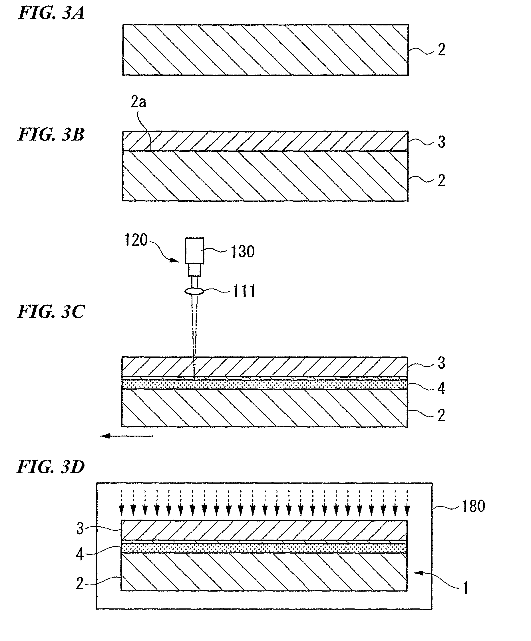
[0169]As described above, according to the present invention, the irradiation position of the condensing point (focal point) G of the laser beam Q2 obtained by converging the laser beam Q1 is set in any micro-region inside the single crystal wafer 2. It is possible to form the gettering sink 4 in any micro-region of the single crystal wafer 2 by reforming the crystal structure of such a micro-region.

[0170]In the laser beam for forming the gettering sinks 4, it is important to set a condition capable of reliably transmitting the laser beam without reforming the crystal structure of the epitaxial layer 3 or the single crystal wafer 2 in the optical path before the laser beam arrives at the condensing point (focal point). Such an irradiation condition of the laser beam is determined by a forbidden band (an energy band gap) which is a basic material property of the semiconductor material. For example, since the forbidden band of a silicon semiconductor is 1.1 eV, when the incident wavel...

third embodiment

[0194]FIG. 14 is a schematic diagram illustrating an apparatus for manufacturing a semiconductor device according the present invention, i.e., an example of a laser irradiation apparatus for forming a gettering sink on a semiconductor wafer. The laser irradiation apparatus (an apparatus for manufacturing a semiconductor device) 320 has a laser irradiator 321 for irradiating laser beams onto the semiconductor substrate 1 along a plurality of optical axes C parallel with one another from the irradiation surface 321a.

[0195]The laser irradiator 321 is formed, for example, in an approximately disc shape having an approximately circular bottom surface greater than or equal to the single crystal wafer 2. Along the irradiation surface 321a facing the single crystal wafer 2, a plurality of laser sources such as laser diodes 315 are provided.

[0196]As shown in FIG. 15, the laser diodes 315 are regularly arranged to be spread over an approximately circular irradiation surface 321a. The positio...


PUM

PropertyMeasurementUnit
temperatureaaaaaaaaaa
wavelengthaaaaaaaaaa
diameteraaaaaaaaaa

Abstract

A method for manufacturing a semiconductor substrate dedicated to a semiconductor device, in which multi-photon absorption is generated in a micro-region inside the semiconductor substrate by condensing laser beams in any micro-region inside the semiconductor substrate, and a gettering sink is formed by changing the crystal structure of only the micro-region.

Description

BACKGROUND OF THE INVENTION[0001]1. Field of the Invention[0002]The present invention relates to a method for manufacturing a semiconductor substrate dedicated to a semiconductor device, an apparatus for manufacturing a semiconductor substrate dedicated to a semiconductor device, a method for manufacturing a semiconductor device, and an apparatus for manufacturing a semiconductor device. Particularly, the present invention relates to a technology for readily forming a gettering site having a certain shape within a short time.[0003]Priority is claimed on Japanese Patent Application No. 2009-133180, filed Jun. 2, 2009, No. 2009-136024, filed Jun. 5, 2009, and No. 2009-136362, filed Jun. 5, 2009, the content of which is incorporated herein by reference.[0004]2. Description of Related Art[0005]Recently, as electronics such as mobile phones and digital video cameras have been remarkably miniaturized, semiconductor devices such as semiconductor memory integrated into the electronics are a...

Claims


Application Information

Patent Timeline
Patent Type & Authority Patents(United States)
IPC IPC(8): H01L21/332
CPCB23K26/0042H01L21/3225H01L21/268B23K26/0635B23K26/0006B23K26/0624B23K2103/56
Inventor KURITA, KAZUNARI
Owner SUMCO CORP
Why Eureka
Try Eureka