AMOLED array substrate and display device

An array substrate and array technology, applied in the field of AMOLED array substrates and display devices, can solve the problems of reduced aperture ratio, organic light-emitting layer, and light-emitting area of ​​display devices, etc., to achieve a large aperture ratio and reduce the aperture ratio Effect, the effect of simple production process

Active Publication Date: 2014-04-09
BOE TECH GRP CO LTD
View PDF3 Cites 37 Cited by
  • Summary
  • Abstract
  • Description
  • Claims
  • Application Information

AI Technical Summary

Problems solved by technology

However, it is necessary to lay several cathode auxiliary lines 120 on the edge of the pixel area (display area), and to form strip-shaped via hol

Method used


Image

  • AMOLED array substrate and display device
  • AMOLED array substrate and display device
  • AMOLED array substrate and display device

Examples


Example Embodiment

[0026] The specific embodiments of the present invention will be described in further detail below in conjunction with the drawings and embodiments. The following examples are used to illustrate the present invention, but not to limit the scope of the present invention.

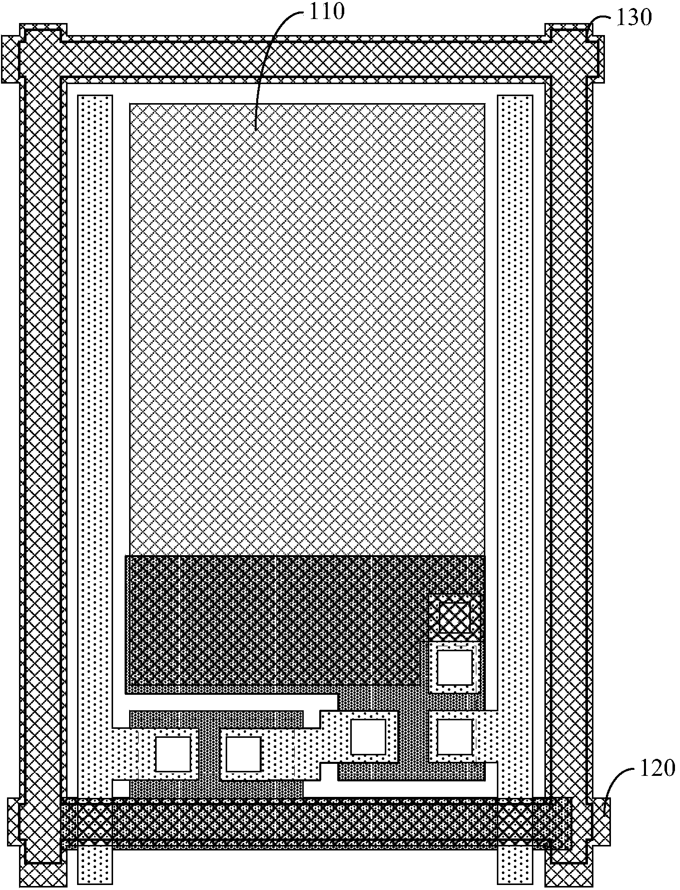
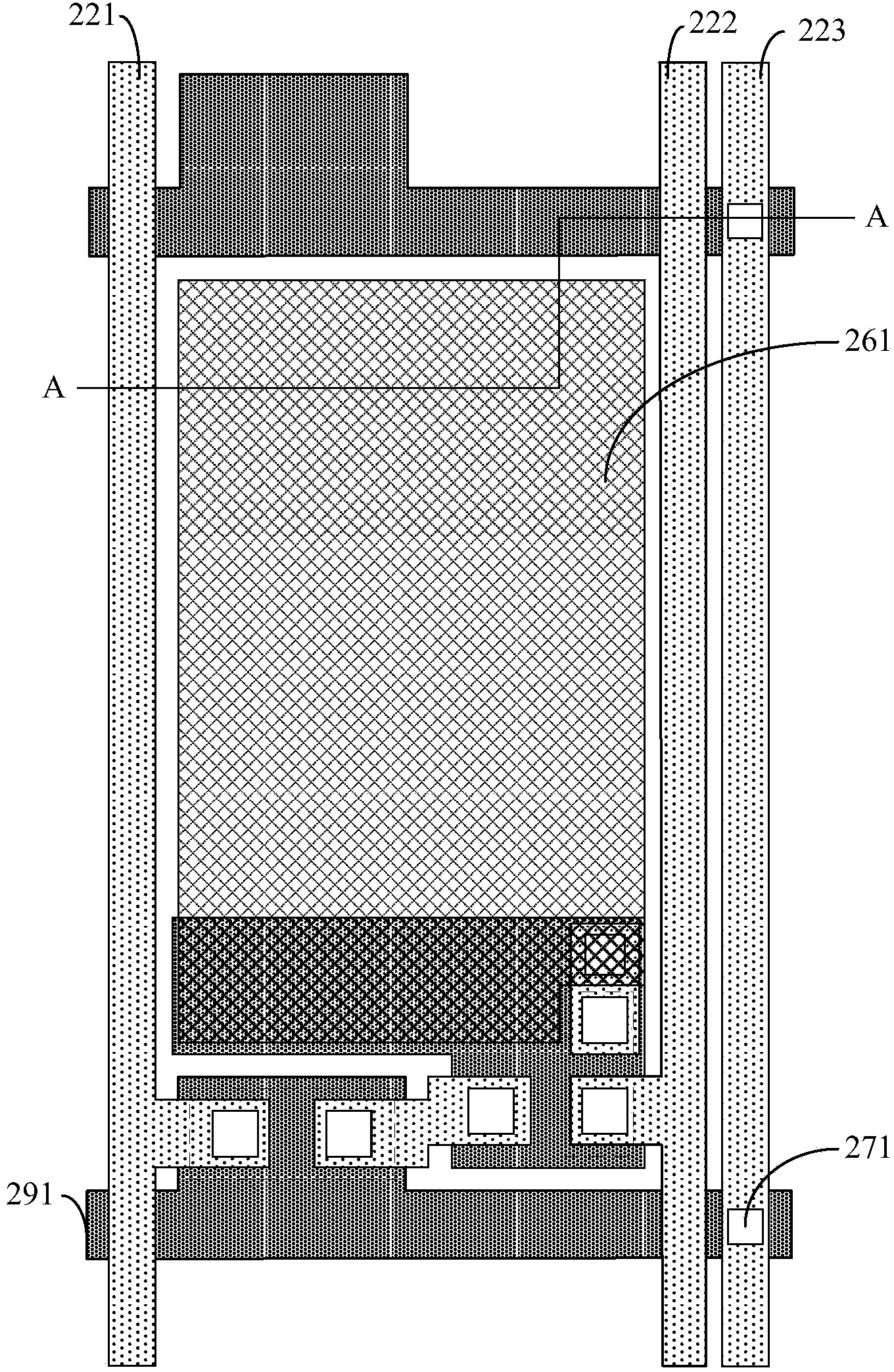
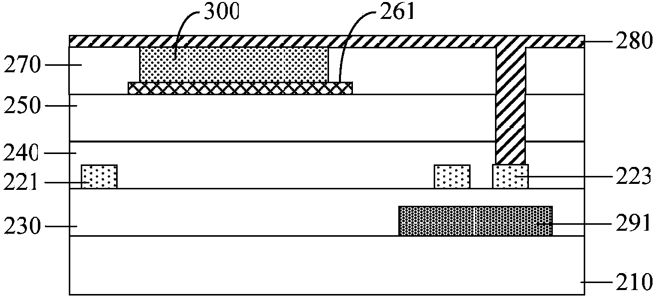
[0027] Such as Figure 2a with 2b As shown, the AMOLED array substrate of the present invention includes several pixel structures formed in an array on a base substrate 210. Each pixel structure is surrounded by a gate line 291 and a signal line 221 and a power supply 222 perpendicular to the gate line 291. Each pixel structure includes a thin film transistor structure, an anode 261, a cathode 280, and an organic light emitting layer 300 between the anode 261 and the cathode 280. Specific hierarchical structure such as Figure 2a with 2b As shown, from bottom to top, it includes: base substrate 210, gate metal layer (including: gate line 291, gate of thin film transistor), gate insulating layer 230, source and ...


PUM


Abstract

The invention discloses an AMOLED array substrate. The AMOLED array substrate comprises a plurality of pixel structures formed in an array mode on a substrate base plate, wherein each pixel structure is defined by a grid line, a signal line and a power line, and the signal line and the power line are perpendicular to the grid line. Each pixel structure comprises a thin film transistor structure, a positive electrode, a negative electrode and an organic luminous layer between the positive electrode and the negative electrode, wherein the positive electrode is located in a region corresponding to each pixel structure, and the negative electrode is a transparent electrode covering the whole substrate base plate. Each pixel structure further comprises a first negative electrode auxiliary line parallel to the signal line, wherein the first negative electrode auxiliary line is connected with the negative electrode through at least two dotted first through holes. In the AMOLED array substrate, each negative electrode is connected with the corresponding first negative electrode auxiliary line on the same layer with the corresponding signal line through the at least two dotted first through holes to enable each negative electrode and the corresponding first negative electrode auxiliary line to be connected in parallel, and the negative electrode resistance is reduced. In addition, the width of each first negative electrode auxiliary line can be decreased, the influence on the opening rate is reduced, and the opening rate is improved compared with the prior art.

Description

technical field [0001] The invention relates to the field of display technology, in particular to an AMOLED array substrate and a display device. Background technique [0002] For a top-emitting AMOLED display device, the cathode is formed by a transparent electrode (such as: ITO), and it is a block electrode covering the array substrate as a whole, so the resistance of the cathode is very high. The cathode resistance is very high, which will increase the IR drop. Excessive IR drop will affect the uniformity of the picture. In order to reduce IR drop, cathode auxiliary lines are used in existing solutions to reduce IR drop, such as figure 1 As shown, in the non-pixel area on the array substrate, several cathode auxiliary lines located on different layers from the cathode are formed, usually at the same time as the anode and / or gate line (or signal line), as shown in figure 1 The middle cathode auxiliary line 120 and the anode 110 are made of the same material and formed at...

Claims


Application Information

Patent Timeline
IPC IPC(8): H01L27/12H01L27/32
Inventor 永山和由
Owner BOE TECH GRP CO LTD
Why Eureka
Try Eureka