

amoled display device
A technology of display device and opposing substrate, which is applied to electrical components, electric solid-state devices, circuits, etc., can solve the problems such as the reduction of the aperture ratio of the display device, and achieve the effect of reducing cathode resistance and reducing IRdrop.
- Summary
- Abstract
- Description
- Claims
- Application Information
AI Technical Summary
Problems solved by technology
Method used
Image

Examples
Embodiment 1
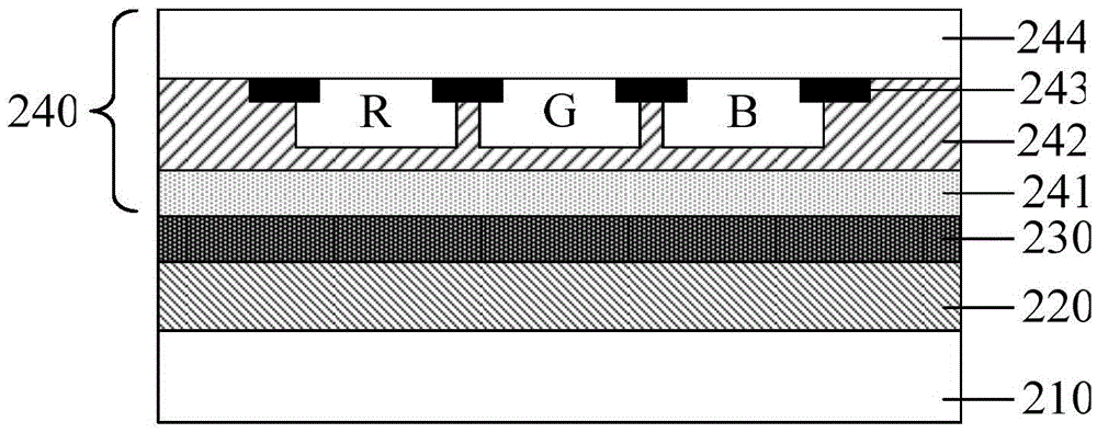
[0025] The AMOLED display device of this embodiment is as Figure 2a As shown, it includes: an array substrate 210 and a substrate opposite to the array substrate 210 . The opposite substrate can be a color filter substrate 240, and the color filter substrate 240 includes: a base substrate 244, a color filter (R, G, B three-color filter) located on the base substrate 244, and a color filter located on the base substrate 244. between the black matrix 243 . The black matrix 243 usually has a mesh structure and is formed in the non-pixel area. The color filter and the black matrix 243 are also covered with a protection layer 242 for protecting the color filter. The light-transmitting conductive structure is a transparent electrode 241 (usually made of Indium Tin Oxide, referred to as ITO) located on the surface of the color filter substrate 240 facing the array substrate 210, that is, the transparent electrode is located on the surface of the protective layer 242 facing the arr...
Embodiment 2
[0029] The AMOLED display device of this embodiment is as Figure 2b As shown, it includes: an array substrate 210 and a substrate opposite to the array substrate 210 . The opposite substrate can be a color filter substrate 240, and the color filter substrate 240 includes: a base substrate 244, a color filter (R, G, B three-color filter) located on the base substrate 244, and a color filter located on the base substrate 244. between the black matrix 243 . The color filter and the black matrix 243 are also covered with a protection layer 242 for protecting the color filter. In this embodiment, the black matrix 243 is made of conductive material (such as metal) and has a mesh structure, so the black matrix 243 can be directly used as a light-transmitting conductive structure connected in parallel with the cathode (that is, the transparent electrode in Embodiment 1 is not required).
[0030] In order to form a parallel structure between the black matrix 243 and the cathode (not...
Embodiment 3
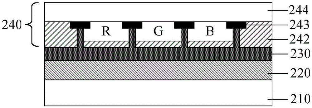
[0033] The AMOLED display device of this embodiment is as Figure 2cAs shown, it includes: an array substrate 210 and a substrate opposite to the array substrate 210 . The opposite substrate can be a color filter substrate 240, and the color filter substrate 240 includes: a base substrate 244, a color filter (R, G, B three-color filter) located on the base substrate 244, and a color filter located on the base substrate 244. between the black matrix 243 . The color filter and the black matrix 243 are also covered with a protection layer 242 for protecting the color filter. In this embodiment, the black matrix 243 is a conductive material (such as metal) and has a mesh structure. It also includes a transparent electrode 241 (usually made of Indium Tin Oxide, referred to as ITO) located on the surface of the color filter substrate 240 facing the array substrate 210 , that is, the transparent electrode is located on the surface of the protective layer 242 facing the array substr...
PUM
 Abstract
Description
Claims
Application Information