Display substrate, display device and preparation method thereof

A technology for display substrates and display devices, which is applied in semiconductor/solid-state device manufacturing, diodes, organic semiconductor devices, etc., and can solve problems such as reducing the resistance of transparent cathodes and reducing the thickness of boxes

Pending Publication Date: 2021-07-23
BOE TECH GRP CO LTD
View PDF5 Cites 1 Cited by
  • Summary
  • Abstract
  • Description
  • Claims
  • Application Information

AI Technical Summary

Problems solved by technology

At present, the top-emitting device can be realized by laminating the display backplane and the color filter cover, but in this process, there a

Method used


Image

  • Display substrate, display device and preparation method thereof
  • Display substrate, display device and preparation method thereof
  • Display substrate, display device and preparation method thereof

Examples


Embodiment Construction

[0030] Embodiments of the present invention are described in detail below. The embodiments described below are exemplary only for explaining the present invention and should not be construed as limiting the present invention. If no specific technique or condition is indicated in the examples, it shall be carried out according to the technique or condition described in the literature in this field or according to the product specification. The reagents or instruments used were not indicated by the manufacturer, and they were all commercially available conventional products.

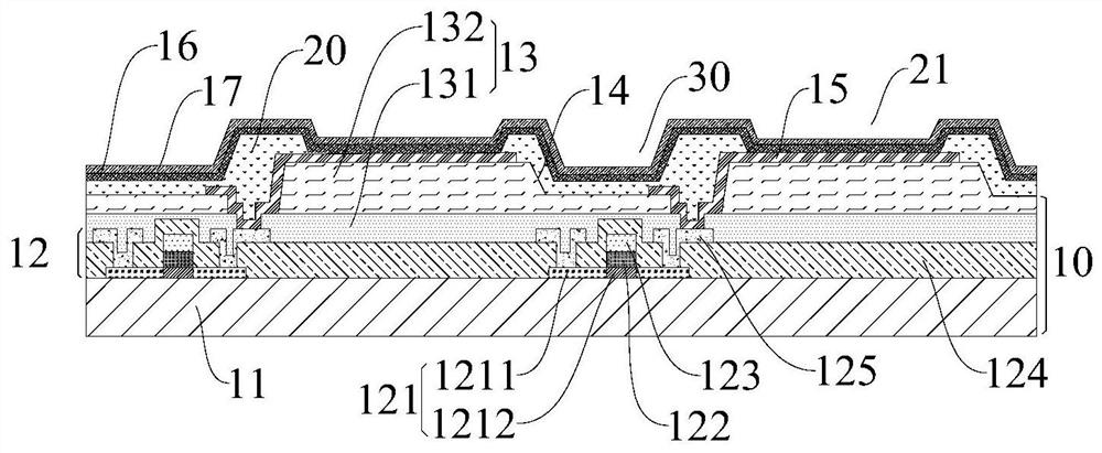
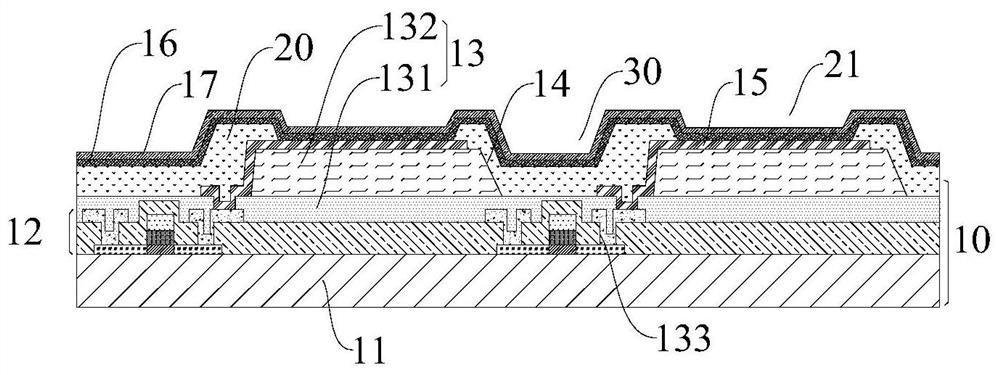
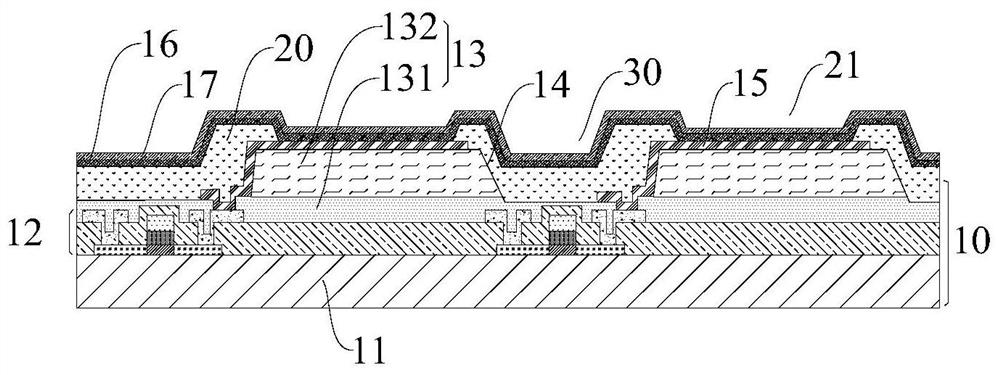
[0031] In one aspect of the present invention, the present invention provides a display substrate. According to an embodiment of the present invention, refer to figure 1 , the display substrate includes: a substrate 10; a pixel defining layer 20, the pixel defining layer 20 is arranged on the substrate 10, and defines a plurality of sub-pixel openings 21; wherein, the side of the display substrate away f...


PUM


Abstract

The invention provides a display substrate, a display device and a preparation method thereof. The display substrate comprises a substrate and a pixel defining layer, wherein the pixel defining layer is arranged on the substrate, and a plurality of sub-pixel openings are defined by the pixel defining layer; and the surface of the side, which is away from the substrate, of the display substrate is provided with at least one concave part, and the orthographic projection of the concave part on the substrate is not overlapped with the orthographic projection of the sub-pixel opening on the substrate. When the display substrate is assembled into a display device, a spacer on a color film substrate can be accommodated in the concave part, so that the thickness of the display device can be greatly reduced, the light emitting path of a light-emitting element can be reduced, the light emitting efficiency of the light-emitting element can be improved, and the service life of the light-emitting element can be prolonged.

Description

technical field [0001] The present invention relates to the field of display technology, in particular, to a display substrate, a display device and a preparation method thereof. Background technique [0002] OLEDs (Organic Light Emitting Diode) are mainly divided into two different structures according to the direction in which light is emitted from the device: one is a bottom-emitting device, and the other is a top-emitting device. In a top-emitting device, light exiting from the top of the device is not affected by TFT (thin film transistor), and the aperture ratio can theoretically reach 100%, which is beneficial to the integration of devices and circuits. At present, the top-emitting device can be realized by laminating the display backplane and the color filter cover, but in this process, many technological problems are faced, such as how to reduce the resistance of the transparent cathode and how to reduce the thickness of the box. [0003] Therefore, current OLEDs-r...

Claims


Application Information

Patent Timeline
IPC IPC(8): H01L27/32H01L51/52H01L51/56
CPCH10K59/38H10K59/12H10K50/824H10K2102/3026H10K71/00H01L27/1214H10K59/123H10K59/122H10K50/865H10K59/1201H10K59/124H10K59/1213
Inventor 王国英徐攀张星韩影高展宋振
Owner BOE TECH GRP CO LTD
Why Eureka
Try Eureka