OLED array substrate and manufacturing method thereof, packaging structure, display device

A technology of array substrate and packaging structure, which is applied in the direction of organic semiconductor devices, semiconductor devices, electrical components, etc., can solve problems such as poor cathode bonding, and achieve the effects of reducing cathode resistance, improving poor bonding, and reducing power consumption

Active Publication Date: 2017-06-23
BOE TECH GRP CO LTD
View PDF5 Cites 0 Cited by
  • Summary
  • Abstract
  • Description
  • Claims
  • Application Information

AI Technical Summary

Problems solved by technology

[0005] The technical problem to be solved by the present invention is to provide an OLED array substrate and its manufacturing method, an OLED packaging structure, and a display device, which can improve the problem of poor cathode lapping on the premise of ensuring the transmittance of the OLED array substrate, and reduce the cost of the OLED array substrate. power consumption

Method used


Image

  • OLED array substrate and manufacturing method thereof, packaging structure, display device
  • OLED array substrate and manufacturing method thereof, packaging structure, display device
  • OLED array substrate and manufacturing method thereof, packaging structure, display device

Examples


Embodiment 1

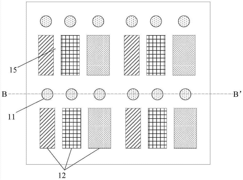
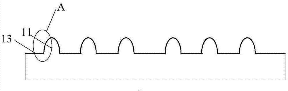
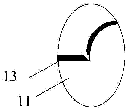
[0036] figure 1 is a schematic plan view of an existing OLED array substrate, figure 2 for figure 1 Schematic diagram of the cross-section in the direction of BB', image 3 for figure 2 An enlarged schematic view of part A in Fig.

[0037] A thin film transistor, a pixel defining layer, an anode, an organic functional layer and a cathode are formed on the OLED array substrate, and the boundary 15 of the pixel defining layer defines a plurality of sub-pixels 12 . Existing top-emitting OLED devices generally require a thinner cathode 13 to ensure higher light transmittance, but since the OLED array substrate needs to be packaged with the packaging substrate, it is also necessary to set a support box thicker on the OLED array substrate. spacer 11, the height of the spacer 11 is mainly composed of the planarization layer resin and the pixel definition layer resin formed before forming the cathode, and the cathode 13 is covered on the spacer 11. Since the spacer 11 has a cer...

Embodiment 2

[0043] The present invention also provides an OLED encapsulation structure, comprising the above-mentioned OLED array substrate and encapsulation substrate.

[0044] Wherein, the edges of the OLED array substrate and the packaging substrate are bonded and fixed by sealing glue, and the OLED packaging structure further includes a spacer for supporting the thickness of the box between the OLED array substrate and the packaging substrate , the spacer is located inside the sealant.

[0045]Since the spacer has a certain height, the OLED array substrate in the area where the spacer is placed has a large fluctuation. In this embodiment, the thickness of the cathode in the area where the spacer is located is increased without changing the thickness of the cathode in other areas. Therefore, without reducing the transmittance of the cathode in the light-emitting area, the problem of poor overlap of the cathode in the area with large fluctuations can be improved, and the resistance of t...

Embodiment 3

[0047] This embodiment also provides a display device, including the above-mentioned OLED encapsulation structure. The display device may be any product or component with a display function such as a mobile phone, a tablet computer, a television, a monitor, a notebook computer, a digital photo frame, a navigator, and the like.


PUM


Abstract

The invention provides an OLED array substrate, a manufacturing method thereof, a packaging structure, and a display device, and belongs to the field of display technology. Wherein, the OLED array substrate includes a thin film transistor, an anode, a cathode, and an organic light-emitting layer between the anode and the cathode, and the OLED array substrate is also provided with a film for supporting the thickness of the box between the OLED array substrate and the packaging substrate. A spacer, the cathode includes a first region covering the spacer and a second region except the first region, and the thickness of the cathode in the first region is greater than the thickness of the cathode in the second region. The technical solution of the invention can improve the problem of poor cathode overlap and reduce the power consumption of the OLED array substrate under the premise of ensuring the transmittance of the OLED array substrate.

Description

technical field [0001] The invention relates to the field of display technology, in particular to an OLED array substrate and a manufacturing method thereof, an OLED packaging structure, and a display device. Background technique [0002] OLED (Organic Light-Emitting Diode, Organic Light-Emitting Diode) devices have become a very Competitiveness and prospects for next-generation display technologies. The organic light-emitting materials and cathode materials used in OLED devices are particularly sensitive to water and oxygen. Too much humidity or too high oxygen content will affect the service life of OLED devices. [0003] In order to effectively block the influence of water and oxygen on the OLED device, the OLED device needs to be packaged, and the OLED array substrate and the packaging substrate are bonded and fixed with a sealant to achieve a closed device structure and block water and oxygen in the air. In addition, a spacer for supporting the thickness of the cell i...

Claims


Application Information

Patent Timeline
Patent Type & Authority Patents(China)
IPC IPC(8): H01L27/32
CPCH10K59/12H10K50/822H10K50/8428H10K50/841H10K2102/351H10K50/82H10K50/8426H10K59/122H10K71/60
Inventor 孙亮
Owner BOE TECH GRP CO LTD
Why Eureka
Try Eureka