

Method for manufacturing high-k metal-gate (HKMG) device
A technology of high dielectric layer and manufacturing method, which is applied in the direction of semiconductor/solid-state device manufacturing, electrical components, semiconductor devices, etc., can solve the problem of high difficulty in process realization, and achieve the effect of reducing uncontrollability and process difficulty
- Summary
- Abstract
- Description
- Claims
- Application Information
AI Technical Summary
Problems solved by technology
Method used
Image

Examples
Embodiment Construction
[0024] The principles and features of the present invention are described below in conjunction with the accompanying drawings, and the examples given are only used to explain the present invention, and are not intended to limit the scope of the present invention.
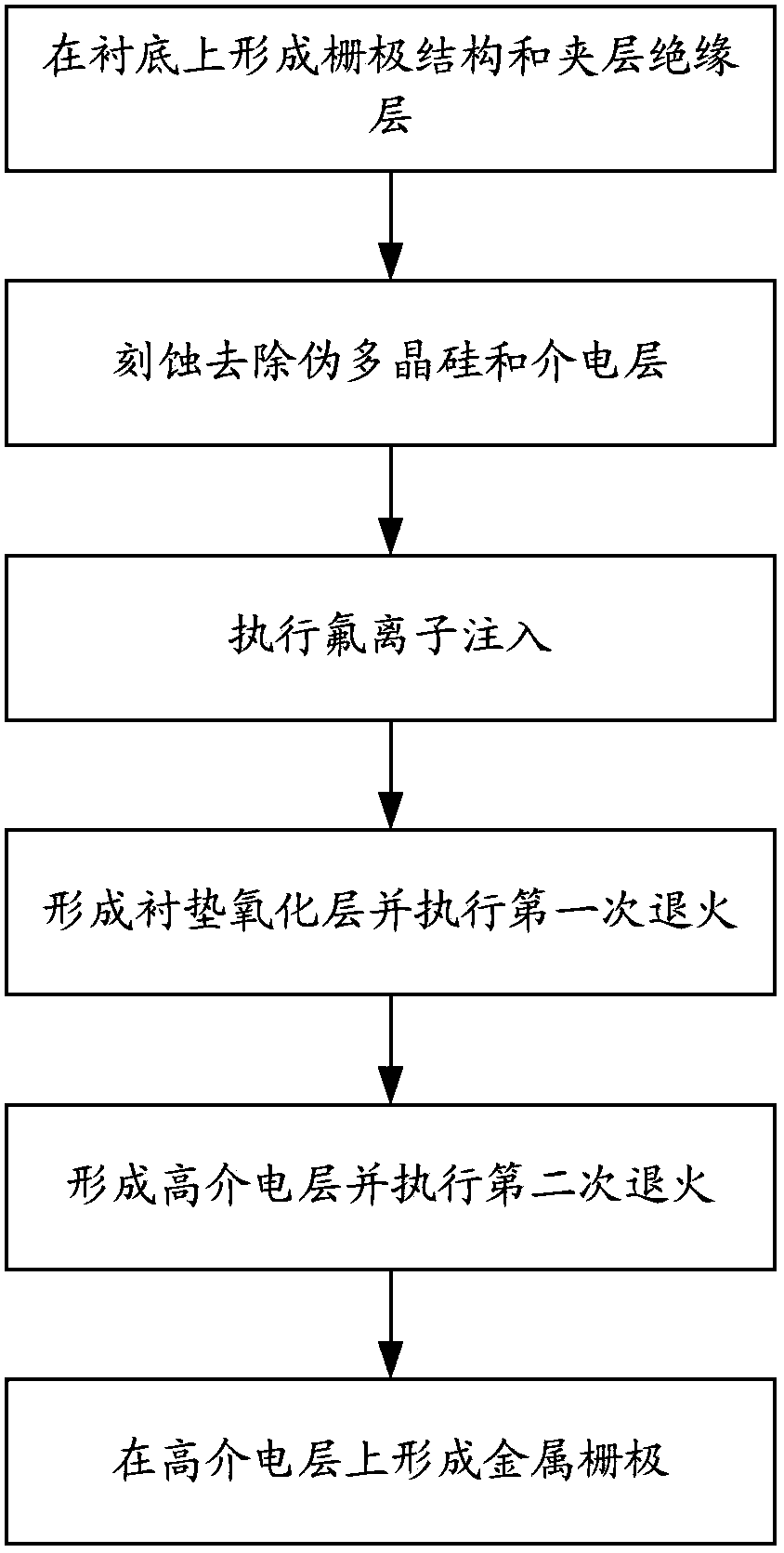
[0025] Such as figure 1 As shown, the present invention provides a method for manufacturing a high dielectric layer metal gate device, comprising:
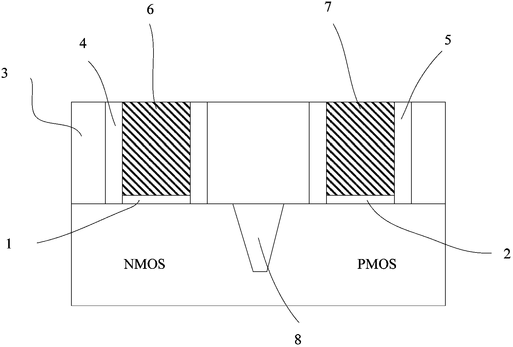
[0026] forming a gate structure including a dielectric layer, dummy polysilicon and sidewall oxide layers on the substrate;
[0027] depositing an interlayer insulating layer on the substrate, and performing chemical mechanical polishing to expose the pseudo-polysilicon;
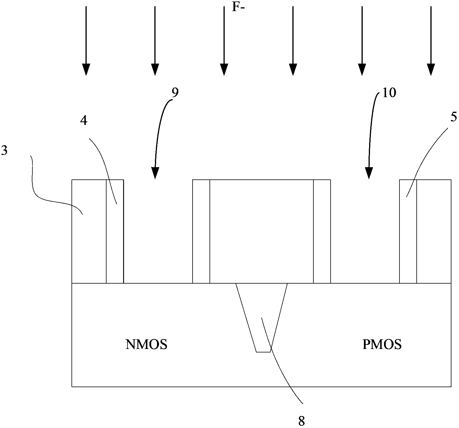
[0028] Etching and removing the dummy polysilicon and the dielectric layer to form a groove whose bottom exposes the substrate corresponding to the dummy polysilicon;
[0029] performing fluorine ion implantation to dope the exposed substrate;
[0030] forming a pad oxide layer at the bottom of the...
PUM
 Abstract
Description
Claims
Application Information