
Photovoltaic system and connector for a photovoltaic cell with interdigitated contacts

A technology for photovoltaic cells and contact parts, which is applied to the assembly of connectors, making the connectors, and the field of connectors, which can solve the problems of not being able to ensure that the openings will face the photovoltaic cells

Inactive Publication Date: 2014-06-04
STICHTING ENERGIEONDERZOEK CENT NEDERLAND
View PDF8 Cites 4 Cited by
  • Summary
  • Abstract
  • Description
  • Claims
  • Application Information

AI Technical Summary

Problems solved by technology

But when the strap is supplied to the photovoltaic cell without preventing twisting of the strap (for example, from the shaft), there is no guarantee that the opening will face the photovoltaic cell

Method used


Image

  • Photovoltaic system and connector for a photovoltaic cell with interdigitated contacts
  • Photovoltaic system and connector for a photovoltaic cell with interdigitated contacts
  • Photovoltaic system and connector for a photovoltaic cell with interdigitated contacts

Examples


Embodiment Construction

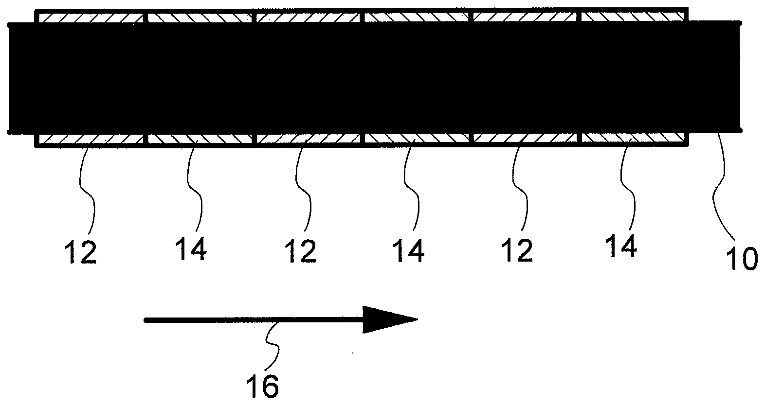
[0029] figure 1 A cross-section of a connection strap for connection to a contact region of a photovoltaic cell is shown. The connection strip (not to scale) comprises an elongated metal core 10 on which is located an insulating coil in the form of a ring 12 of electrically insulating material at positions in the axial direction 16 of the core 10, separated from each other by a solder ring 14 of solder . In cross-section, each insulating ring 12 and each solder ring 14 are shown as two regions, but it is understood that each insulating ring 12 and each solder ring 14 may extend around the core 10 along a circumferential path.

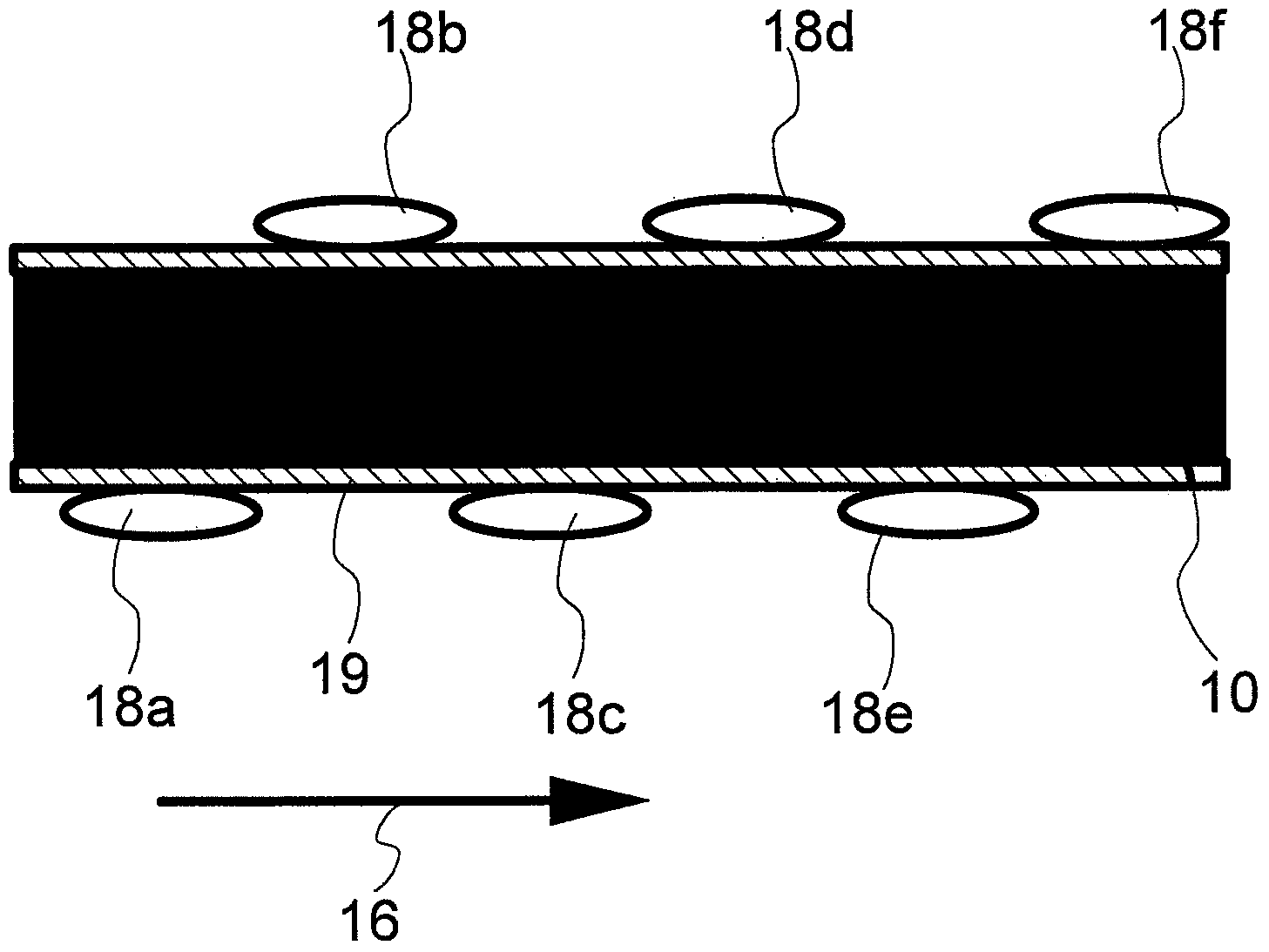
[0030] Figure 1a A cross-section through an alternative connection strap for connection to the contact regions of a photovoltaic cell is shown. In this embodiment the coils are part of a strip 18a - f of electrically insulating material which extends helically around the metal core 10 . ("helically" is known to mean a curve corresponding to the hel...


PUM


Abstract

A photo-voltaic cell system has a semi-conductor substrate having a surface with interdigitated first and second contact areas thereon, providing contact to emitter and base contact areas in or on the semi-conductor. A connection string comprises a conductor line and electrically isolating material in rings around the conductor line. Parts of the conductor line between the rings are joined to a plurality of the first contact areas, in electrical contact with the first contact areas, with electrically isolating material from the rings between the conductor line and the second contact areas.

Description

technical field [0001] The invention relates to a photovoltaic system with an interdigitated back contact (IBC) design, to a connector suitable for use as a conductive connector for an electrical contact area in a photovoltaic system, and to a A connector assembly and a method for making the connector. Background technique [0002] Photovoltaic cells are designed as semiconductor devices that convert photons into electricity. A well known use is its use as a solar panel (see eg US 4,234,352). Typically, photovoltaic cells include semiconducting materials as photosensitizing materials in which light energy (photons) is converted into excited mobile charge carriers. Semiconducting materials typically have a p-n junction as defined herein. In planar cells, p-n junctions are usually formed near the surface of semiconducting materials. The conductors on the p-regions and n-regions on the surface of the semiconducting material form the contacts (also called contact regions) fo...

Claims


Application Information

Patent Timeline
Patent Type & Authority Applications(China)
IPC IPC(8): H01L31/05H01L31/18
CPCH01L31/05Y02E10/50
Inventor 伊尔卡伊·赛萨尔马库斯·约翰·扬森
Owner STICHTING ENERGIEONDERZOEK CENT NEDERLAND
Learn More