Integrated circuit on-chip communication method and device based on three physical interconnection lines

A technology of integrated circuits and communication methods, applied in electrical digital data processing, instruments, etc., can solve the problems of DCR bus physical connections, inaccessible slave devices, occupying large wiring resources, etc., to achieve less hardware resources and physical implementation costs. , The effect of reducing the occupancy of global routing resources and the number of long signal lines

Active Publication Date: 2016-08-31
NAT UNIV OF DEFENSE TECH
View PDF3 Cites 0 Cited by
  • Summary
  • Abstract
  • Description
  • Claims
  • Application Information

AI Technical Summary

Problems solved by technology

However, when multiple slave devices are cascaded, the address bus and data bus structure of the master device and each slave device must be arranged separately, and the number of interconnection lines is large, so the increase in the number of slave devices will inevitably lead to time-consuming physical implementation. Occupies a large number of routing resources, increasing the difficulty of timing constraints during physical implementation
Moreover, the DCR bus structure cannot support low-power technologies such as power-off. Once a node in the cascaded node is powered off, all accesses to its subsequent nodes will not be possible.
[0004] To sum up, the daisy chain DCR bus has the following problems: (1) The address, data, control and other signals of the DCR bus have separate physical connection lines, resulting in many physical connections of the entire DCR bus, occupying a large amount of wiring resources, increased chip area
Moreover, there is a timing relationship between each group of interconnect lines, which must be constrained in the physical design, which increases the difficulty and complexity of the physical design; (2) On the slave device chain of the DCR bus, a slave device that is powered off will cause All subsequent slave devices are inaccessible, so low-power management technologies such as flexible device power-off are not supported

Method used


Image

  • Integrated circuit on-chip communication method and device based on three physical interconnection lines
  • Integrated circuit on-chip communication method and device based on three physical interconnection lines
  • Integrated circuit on-chip communication method and device based on three physical interconnection lines

Examples


Embodiment Construction

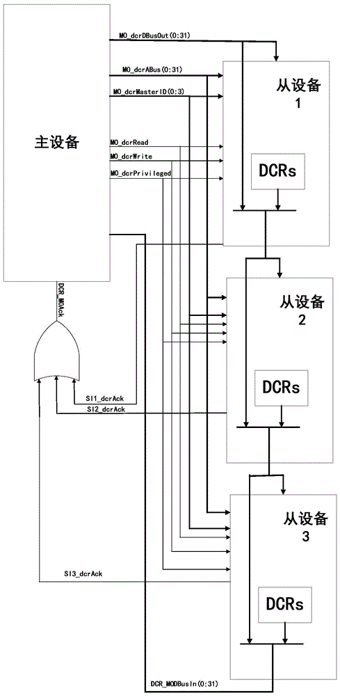
[0029] Such as figure 2 As shown, the implementation steps of the integrated circuit on-chip communication method based on three physical interconnection lines in this embodiment are as follows:

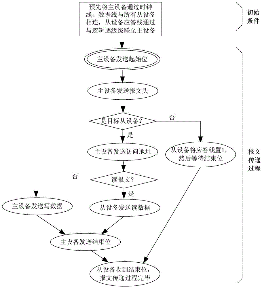
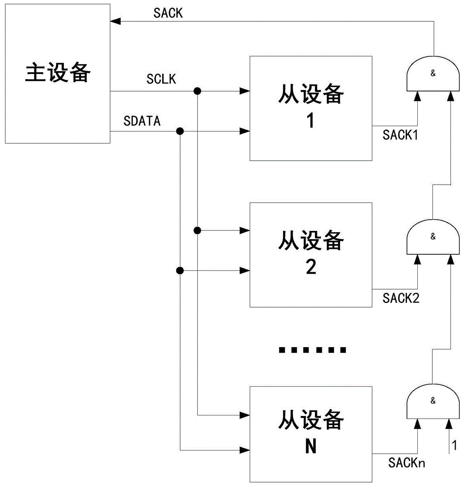
[0030] 1) Connect the clock output interface of the master device to each slave device through a clock line in advance, connect the data interface of the master device to each slave device through a data line, and connect the response lines of each slave device through the After logically cascading, it is finally connected to the response interface of the master device; when the master device sends a message to the slave device, it divides the message into five micro In the micropacket transmission process, each slave device synchronizes with the master device through the clock line of the master device, and the timing of each slave device exchanging data and responding is completely determined by the clock sent by the master device; the master device passes the clock line, data Th...


PUM


Abstract

The invention discloses an on-chip communication method on the basis of three physical interconnection lines for integrated circuits. The on-chip communication method includes preliminarily connecting a master with slaves by clock lines and data lines, cascading acknowledgment lines of the various slaves step by step by the aid of AND logics and finally connecting the acknowledgment lines with an acknowledgment interface of the master; segmenting each message into five micro-packets including a start bit, a message header, an address, a data volume and a stop bit when the message is transmitted from the master to the corresponding slave, sequentially transmitting each five corresponding micro-packets including the start bit, the message header, the address, the data volume and the stop bit between the master and the corresponding slave, enabling the slaves to receive the messages comprising the multiple micro-packets from the master via the clock lines and the data lines in transmission procedures, enabling the slaves to transmit acknowledgment and message read return data to the master via the acknowledgment lines, and enabling the slaves to receive message write data via the data lines. The message write data are transmitted from the master. The on-chip communication method has the advantages of few interconnection lines and occupied hardware resources and capability of supporting flexible slave power shut-off strategies.

Description

technical field [0001] The invention relates to the on-chip communication field of an integrated circuit SOC chip, in particular to an integrated circuit on-chip communication method and device based on three physical interconnection lines. Background technique [0002] SOC chip design has become the mainstream in the field of chip design, especially in the field of embedded mobile communication. Generally, many components are integrated on the SOC chip, such as SDRAM controller, USB, PCIE, SATA, UART, SPI, SIM card controller and other functional components, often reaching dozens of types. In order to connect many functional components together, people have studied a variety of SOC on-chip bus structures, such as AMBA, CoreConnect, etc. These buses are all synchronous bus types, which have the advantages of high bandwidth and low delay, but require the devices on the bus to belong to The same clock domain or cross-clock conversion, and this type of bus requires more interc...

Claims


Application Information

Patent Timeline
Patent Type & Authority Patents(China)
IPC IPC(8): G06F13/40
Inventor 张明郭御风邓宇龚锐石伟任巨马爱永高正坤窦强
Owner NAT UNIV OF DEFENSE TECH
Why Eureka
Try Eureka