On-chip communication method and device of integrated circuit based on asynchronous structure

An integrated circuit, asynchronous structure technology, applied in the direction of electrical digital data processing, instruments, etc., can solve the problems of not supporting information transmission, increasing the chip area and physical implementation difficulty, occupying wiring resources, etc., to achieve strong scalability, reduce physical Realization difficulty and the effect of reducing the occupancy of hardware resources

Active Publication Date: 2013-03-20
NAT UNIV OF DEFENSE TECH
View PDF3 Cites 17 Cited by
  • Summary
  • Abstract
  • Description
  • Claims
  • Application Information

AI Technical Summary

Problems solved by technology

[0005] (1) In the daisy chain DCR bus, when multi-level slave devices are cascaded with the master device, there will be a large number of long communication lines between the master and slave devices, occupying a large amount of wiring resources, increasing the chip area and the difficulty of physical implementation;
[0006] (2) The daisy chain DCR bus only supports read and write information transmission, and does not support other types of information transmission such as slave device interrupts

Method used


Image

  • On-chip communication method and device of integrated circuit based on asynchronous structure
  • On-chip communication method and device of integrated circuit based on asynchronous structure
  • On-chip communication method and device of integrated circuit based on asynchronous structure

Examples


Embodiment Construction

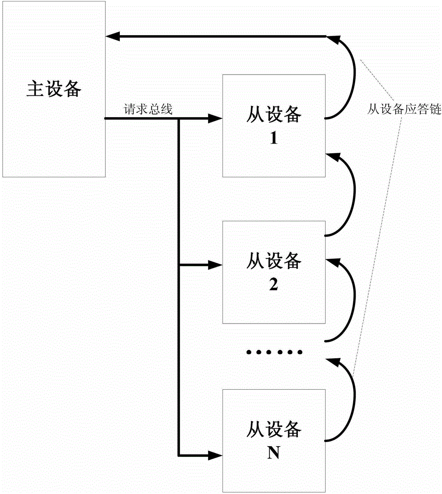
[0030] Such as figure 2 As shown, the implementation steps of the integrated circuit on-chip communication method based on the asynchronous structure in the embodiment of the present invention are as follows:

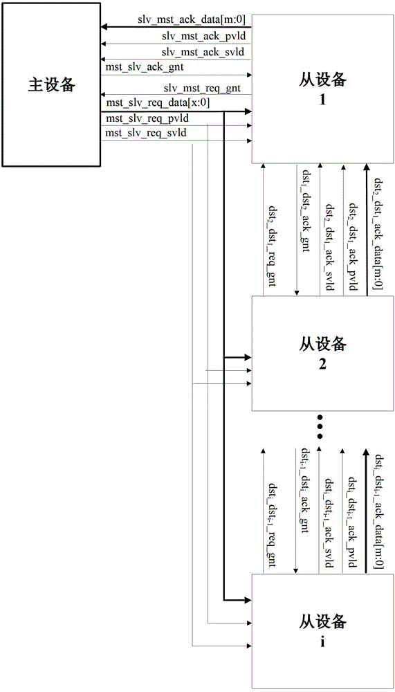
[0031]1) The master device is directly connected to the request interface of each slave device through the request bus in advance, and multiple slave device response interfaces are connected in series in advance to form a slave device response chain, and the slave device response interface located at the head of the slave device response chain is connected to the The master device is connected to the response interface, the slave device receives the request message composed of micropackets from the master device through the request bus, and the slave device sends the response message composed of micropackets to the master device through the slave device response chain;

[0032] 2) When the master device sends a message to the slave device, the master device first divid...


PUM


Abstract

The invention discloses an on-chip communication method and an on-chip communication device of an integrated circuit based on an asynchronous structure. The structure comprises the following steps of 1, directly connecting main equipment to each auxiliary equipment request interface by a request bus in advance, sequentially and serially connecting a plurality of auxiliary equipment response interfaces to form an auxiliary equipment response chain in advance, and connecting the auxiliary equipment response interface on the head of the auxiliary equipment response chain with a main equipment response interface; and 2, when the main equipment communicates with the auxiliary equipment, receiving a request message consisting of a plurality of micro-packets from the main equipment by the auxiliary equipment through the request bus, and sending a response message consisting of the micro-packets to the main equipment by the auxiliary equipment through the auxiliary equipment response chain. The device comprises the main equipment and the auxiliary equipment, wherein the main equipment is directly connected with each auxiliary equipment through the request bus, the auxiliary equipment are sequentially and serially connected to form the auxiliary equipment response chain, and the auxiliary equipment on the head of the auxiliary equipment response chain is connected with the main equipment. The method and the device have the advantages that the number of long signal lines is little, the occupation of hardware resources is little, and the expandability is good.

Description

technical field [0001] The invention relates to the field of on-chip communication of an integrated circuit SOC chip, in particular to a method and device for on-chip communication of an integrated circuit based on an asynchronous structure. Background technique [0002] With the rapid increase in the scale and design complexity of integrated circuit SOC chips, the research on the SOC on-chip bus structure has attracted more and more attention, and a variety of on-chip buses have been developed, such as AMBA, CoreConnect, etc. These buses are all synchronous bus types. It has the advantages of high bandwidth and low delay, but requires that the devices on the bus belong to the same clock domain, and the number of interconnection lines of this type of bus is large, which takes up more hardware resources. However, in integrated circuits, some components do not require high-speed access interfaces, but are more concerned about reducing the occupation of hardware resources and t...

Claims


Application Information

Patent Timeline
Patent Type & Authority Applications(China)
IPC IPC(8): G06F13/38G06F13/42
Inventor 张明郭御风石伟罗莉龚锐邓宇任巨马爱永窦强王永文
Owner NAT UNIV OF DEFENSE TECH
Why Eureka
Try Eureka