Die Bonding Method

A chip bonding and bonding technology, which is applied in the direction of instruments, welding equipment, optical mechanical equipment, etc., can solve problems such as fragmentation and chip bonding offset, and achieve the effect of improving quality, increasing yield, and reducing chip position changes

Active Publication Date: 2018-10-16
SEMICON MFG INT (SHANGHAI) CORP
View PDF5 Cites 0 Cited by
  • Summary
  • Abstract
  • Description
  • Claims
  • Application Information

AI Technical Summary

Problems solved by technology

[0006] The purpose of the present invention is to provide a chip bonding method to solve the problem of chip bonding offset or debris in the prior art, thereby improving the bonding quality

Method used


Image

  • Die Bonding Method
  • Die Bonding Method
  • Die Bonding Method

Examples


Embodiment Construction

[0029] The chip bonding method provided by the present invention will be further described in detail below in conjunction with the accompanying drawings and specific embodiments. Advantages and features of the present invention will be apparent from the following description and claims. It should be noted that all the drawings are in a very simplified form, and are only used for the purpose of conveniently and clearly assisting in describing the embodiments of the present invention.

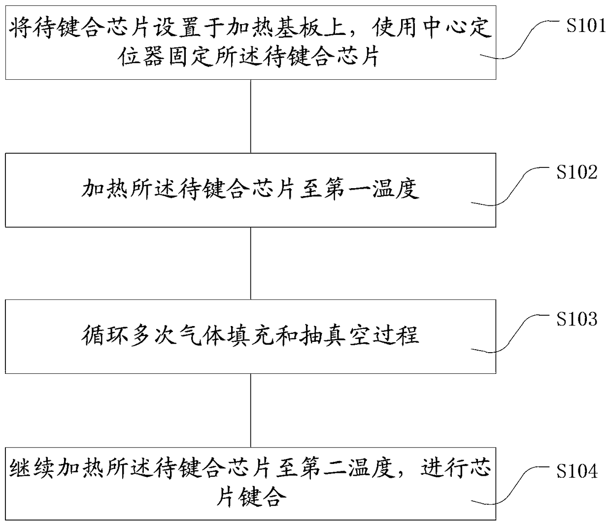
[0030] Please refer to figure 1 In the flow chart provided, the chip bonding method of this embodiment includes the following steps:

[0031] Step S101, placing the chip to be bonded on the heating substrate, and fixing the chip to be bonded with a center locator;

[0032] Step S102, heating the chip to be bonded to a first temperature;

[0033] Step S103, cycle multiple times of gas filling and vacuuming;

[0034] Step S104, continuing to heat the chip to be bonded to a second temperature to...


PUM


Abstract

The invention discloses a chip bonding method. According to the method, when a to-be-bonded silicon chip is heated to certain temperature, the process of gas filling and vacuum pumping is carried out repeatedly to exhaust the gas attached to the chip itself, thereby avoiding formation of cavities after bonding. In addition, the use of a center locator to fix the to-be-bonded chip before heating can effectively limit position offset of the chip and decrease chip position variation caused by changes of temperature, pressure and the like, thus greatly improving the quality of the bonded chip and improving the yield.

Description

technical field [0001] The invention relates to the field of integrated circuit manufacturing, in particular to a chip bonding (bonder) method. Background technique [0002] Micro-Electro-Mechanical Systems (MEMS) is a high-tech cutting-edge discipline developed on the basis of integrating various micro-processing technologies and applying the latest achievements of modern information technology. Compared with traditional machinery, their size Smaller, with excellent electrical performance, the cost performance is greatly improved compared with traditional mechanical manufacturing. [0003] In the MEMS process, silicon-silicon direct bonding and silicon-glass electrostatic bonding are the most commonly used technologies. Recently, a variety of new bonding technologies have been developed, such as metal-metal bonding technology. However, although various technologies continue to However, MEMS is not yet mature, and each technology has certain defects. [0004] The CB8 chip ...

Claims


Application Information

Patent Timeline
Patent Type & Authority Patents(China)
IPC IPC(8): B81C3/00
Inventor 黄平
Owner SEMICON MFG INT (SHANGHAI) CORP
Why Eureka
Try Eureka