A gating circuit and gating method for resistance transition random access memory rram

A random access memory and resistance conversion technology, applied in the field of memory, can solve problems such as high power consumption, insufficient memory speed index, and low resource utilization

Active Publication Date: 2017-02-15
INST OF MICROELECTRONICS CHINESE ACAD OF SCI
View PDF6 Cites 0 Cited by
  • Summary
  • Abstract
  • Description
  • Claims
  • Application Information

AI Technical Summary

Problems solved by technology

[0009] It is not difficult to find that the above gating method is simple in idea and easy to operate, but its disadvantages are also obvious, that is, high power consumption, low resource utilization, and only one storage unit can be selected at the same time
Clearly insufficient for growing memory speed metrics

Method used


Image

  • A gating circuit and gating method for resistance transition random access memory rram
  • A gating circuit and gating method for resistance transition random access memory rram
  • A gating circuit and gating method for resistance transition random access memory rram

Examples


Embodiment 1

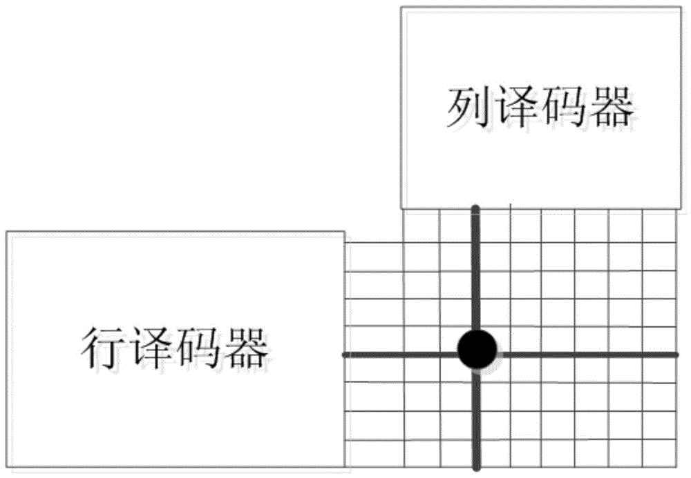
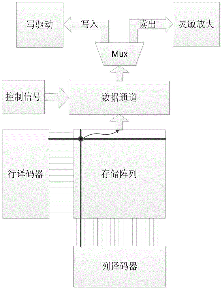
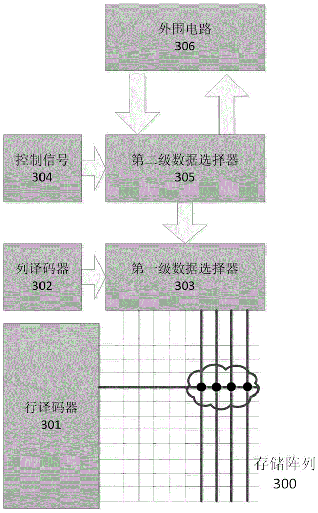
[0029] see image 3 , a gating circuit of a resistance transition random access memory RRAM, comprising: a row decoder 301, a column decoder 302, a first data selector 303 and a second data selector 305; the second data selector 305 is connected to a control signal 304; the control signal includes: a read enable signal and a write enable signal, which are used to select the working mode of the memory, that is, read or write; the second data selector 305 is connected with the first data selector 301 and the RRAM respectively Peripheral circuits 306 are connected to realize data writing and reading of the memory array; wherein, the row decoder 301 receives an external row address signal, sends a row gate signal to the memory array of the RRAM, and gates a row of memory cells; column decoding The device 302 receives an external column address signal, sends a column strobe signal to the first data selector 303, and selects a plurality of columns of memory cells; thus, in the memor...

Embodiment 2

[0039] see Figure 4 , on the basis of Embodiment 1, this embodiment proposes this embodiment for the selection switch and additional structural features; the data selection switch 4031 includes a transmission gate 40311 and an inverter 40312; the control signal terminal of the transmission gate 40311 and the inverter The input terminal of 40312 is connected as the control signal input terminal of data selection switch 4031, and is connected with the output terminal of column decoder 402; the input terminal of transmission gate 40311 is connected with the column line of memory array as the input terminal of data selection switch 4031 ; The output end of the transmission gate 40311 is connected to the second-stage data selector 405 through the data path 404; the output end of the inverter 40312 is connected to the inverting clock of the transmission gate 40311; thereby realizing a stable and efficient gating operation.

Embodiment 3

[0041] Such as Figure 5 As shown, the structure of the resistive memory is basically the same as the structure proposed in the second embodiment; the difference is that the output of the column decoder not only controls one selection switch, but controls n ones at the same time. Moreover, the decoding method of the column decoder is also different from the traditional method, adopting the method of segment decoding and then ANDing.

[0042] Taking the 8-bit data to be decoded as an example, the 8-bit decoded data is divided into bits [0:3] and bits [4:7]. First decode the [0:3] bit data, the result is 2 4 bit, and then decode the [4:7] bit data, the result is 2 4 . Then translate the [0:3] bits to 2 4 bit data respectively and [7:4] bits to translate the 2 4 The bit data is ANDed, and then combined according to the high and low bits, and finally 2 is obtained 8 The bit data is the complete and correct decoding result of the decoder. The input signal of the column decod...


PUM


Abstract

The invention belongs to the technical field of storages and discloses a gating circuit of a resistive random access memory (RRAM). The gating circuit comprises a row decoder, a line decoder, a first data selector and a second data selector, wherein the second data selector is connected with a control signal; the control signal comprises a write enable signal and a read enable signal which are used for selecting operating modes of the selectors, namely reading or writing; the second data selector is respectively connected with the first data selector and a peripheral circuit of the RRAM and is used for reading or writing the data; the row decoder receives an external row gating address signal for address decoding, transmits the signal to a storage array of the RRAM and gates a row of storage units; the line decoder receives an external line gating address signal for address decoding, transmits the signal to the first data selector and gates multiple lines of storage units. The multiple storage units are simultaneously gated, so that the reading / writing speed of the storage unit is improved.

Description

technical field [0001] The invention relates to the technical field of memory, in particular to a gating circuit and a gating method of a resistance transition random access memory (RRAM). Background technique [0002] As human beings enter the information age, the demand for information storage is also getting higher and higher. Massive information not only requires higher storage density, but also puts forward new requirements for the response speed and reliability of the memory. Against this background, the semiconductor industry has been looking for a new type of nonvolatile memory with high speed, high density and low power consumption. The so-called non-volatile means that the random access memory can still retain the stored information even in the case of power failure, which is undoubtedly very important for the security and stability of information storage. [0003] Although the response speed of static random access memory (SRAM) and dynamic random access memory ...

Claims


Application Information

Patent Timeline
Patent Type & Authority Patents(China)
IPC IPC(8): G11C16/06G11C16/26G11C16/02
Inventor 张锋
Owner INST OF MICROELECTRONICS CHINESE ACAD OF SCI
Why Eureka
Try Eureka