Display device

A technology for display devices and substrates, which is applied to static indicators and other directions, can solve the problems of difficult narrow frame design and restrictions, and achieve the effect of narrowing the frame of the display device.

Inactive Publication Date: 2014-12-10
BOE TECH GRP CO LTD +1
View PDF5 Cites 4 Cited by
  • Summary
  • Abstract
  • Description
  • Claims
  • Application Information

AI Technical Summary

Problems solved by technology

[0004] To sum up, it is difficult to realize narrow frame design due to the limitation of the space occupied by the gate drive circuit on the array substrate when designing LCD products using the A-Si process in the prior art
With the development of electronic products such as mobile phones, display screens with narrow bezels have increasingly become an inevitable trend of development. Therefore, the development of traditional A-Si LCD products has been greatly restricted in the development of bezels.

Method used


Image

  • Display device
  • Display device
  • Display device

Examples


Embodiment 1

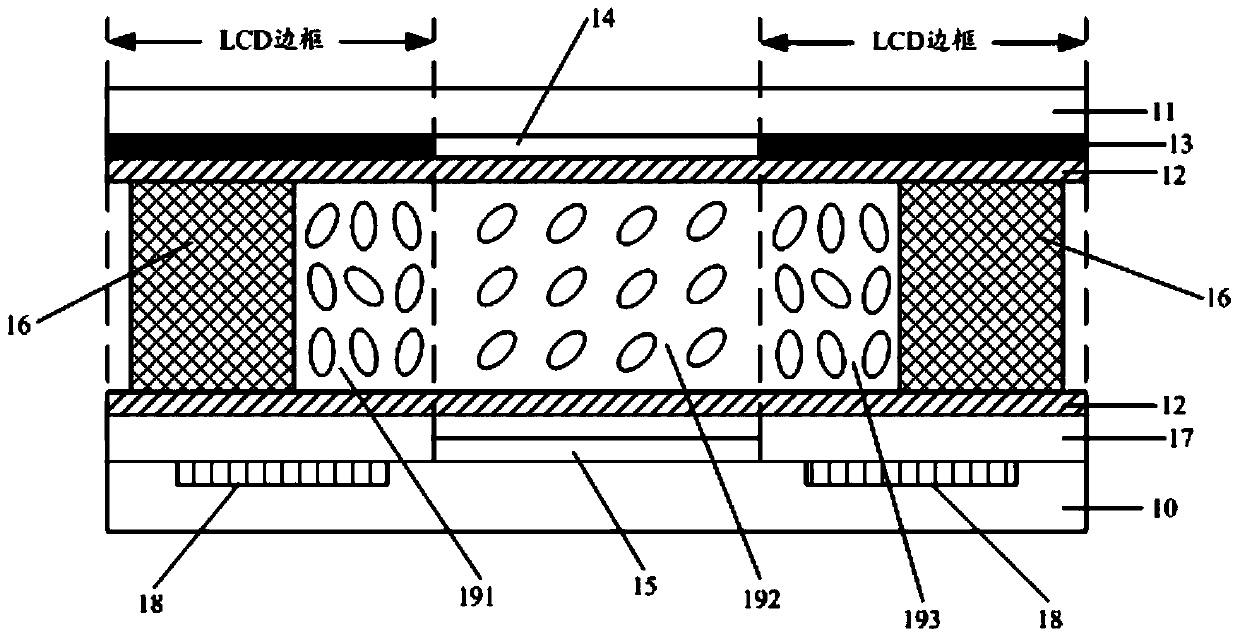
[0043] Such as image 3 As shown, the display device provided by the specific embodiment of the present invention includes: a first substrate 20 and a second substrate 21 oppositely arranged, a liquid crystal molecule 22 and a sealant 27 located between the first substrate 20 and the second substrate 21, and a set The first gate drive circuit 23 on the first substrate 20, the second gate drive circuit 24 arranged on the second substrate 21, the first substrate 20 includes a number of first pixel units 25 arranged in an array, as shown in the figure There are two first pixel units 251 and 252, and the thin film transistors in the first pixel units in each row are connected to the first gate drive circuit 23 through a gate line, such as: the thin film transistors in the first pixel unit 251 in the figure The gate and the gate of the thin film transistor in the first pixel unit 252 are connected to the same gate line, through which the gate line is connected to the first gate dri...

Embodiment 2

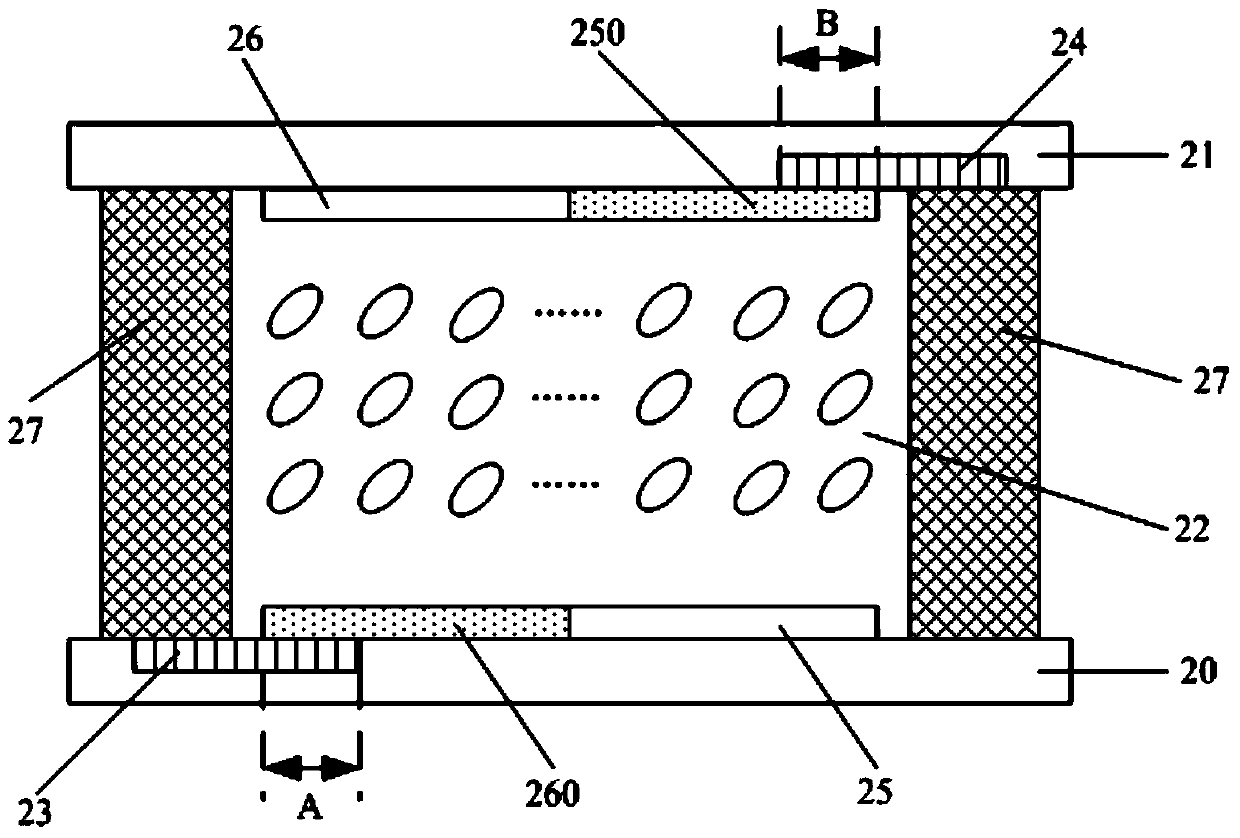
[0050] Such as Figure 4 As shown, the display device provided by the specific embodiment of the present invention includes: a first substrate 20 and a second substrate 21 oppositely arranged, a liquid crystal molecule 22 and a sealant 27 located between the first substrate 20 and the second substrate 21, and a set The first gate drive circuit 23 on the first substrate 20, the second gate drive circuit 24 arranged on the second substrate 21, the first substrate 20 includes a number of first pixel units 25 arranged in an array, as shown in the figure Two first pixel units 251 and 252 are provided, and the thin film transistors in each row of the first pixel units are connected to the first gate drive circuit 23 through a gate line; the second substrate 21 includes several second pixel units 26 arranged in an array , two second pixel units 261 and 262 are shown in the figure, and the thin film transistors in each row of second pixel units are connected to the second gate driving...


PUM


Abstract

The invention discloses a display device which is used for achieving the purpose of decreasing the size of a frame of the display device. The display device comprises a first substrate, a second substrate, a liquid crystal molecule, a first gate drive circuit and a second gate drive circuit. The first substrate and the second substrate are oppositely arranged, the liquid crystal molecule is located between the first substrate and the second substrate, the first gate drive circuit is arranged on the first substrate, and the second gate drive circuit is arranged on the second substrate. The first substrate comprises first pixel units which are arranged in an array mode, and thin film transistors in the first pixel units of the first row are connected with the first gate drive circuit through a gate line. The second substrate comprises second pixel units which are arranged in an array mode, and thin film transistors in the second pixel units of the first row are connected with the second gate drive circuit through a gate line. Part of the projection area of the second pixel units on the first substrate and the arrangement area of the first gate drive circuit have an overlapped area, and part of the protection areas of the first pixel units on the second substrate and the arrangement area of the second gate drive circuit have an overlapped area.

Description

technical field [0001] The present invention relates to the technical field of displays, in particular to a display device. Background technique [0002] The traditional liquid crystal display (Liquid Crystal Display, LCD) using amorphous silicon (A-Si) process such as figure 1 As shown, the LCD includes an array substrate 10 and a color filter substrate 11 oppositely arranged, and a sealant 16 is arranged between the array substrate 10 and the color filter substrate 11 . The gate driver on array (GOA) technology is to integrate the thin film transistor as the gate switch circuit on the array substrate, thereby saving the gate driver integrated circuit part. The GOA 18 in the prior art is respectively arranged on both sides of the array substrate 10, 15 represents the pixel units arranged in an array on the array substrate 10, and the thin film transistors in the pixel units located in the left area of ​​the array substrate 10 in the pixel unit 15 The GOA 18 arranged on th...

Claims


Application Information

Patent Timeline
Patent Type & Authority Applications(China)
IPC IPC(8): G02F1/133
Inventor 吴昊
Owner BOE TECH GRP CO LTD
Why Eureka
Try Eureka