Step-gate dielectric double-layer graphene field-effect transistor and preparation method thereof

A field-effect transistor and double-layer graphene technology, applied in the field of nanoelectronics, can solve the problems of insufficient logic switches, large off-state current, and low switching ratio, and achieve the effect of simple preparation process and suppression of off-state current

Active Publication Date: 2017-02-15
PEKING UNIV
View PDF6 Cites 1 Cited by
  • Summary
  • Abstract
  • Description
  • Claims
  • Application Information

AI Technical Summary

Problems solved by technology

But its switch ratio is generally not higher than 100, which is not enough for logic switch applications
The main reason for the low switching ratio of this structure is the large off-state current

Method used


Image

  • Step-gate dielectric double-layer graphene field-effect transistor and preparation method thereof
  • Step-gate dielectric double-layer graphene field-effect transistor and preparation method thereof
  • Step-gate dielectric double-layer graphene field-effect transistor and preparation method thereof

Examples


Embodiment Construction

[0037] The present invention will be further illustrated by examples below. It should be noted that the purpose of publishing the embodiments is to help further understand the present invention, but those skilled in the art can understand that various substitutions and modifications are possible without departing from the spirit and scope of the present invention and the appended claims. of. Therefore, the present invention should not be limited to the content disclosed in the embodiments, and the scope of protection claimed by the present invention is subject to the scope defined by the claims.

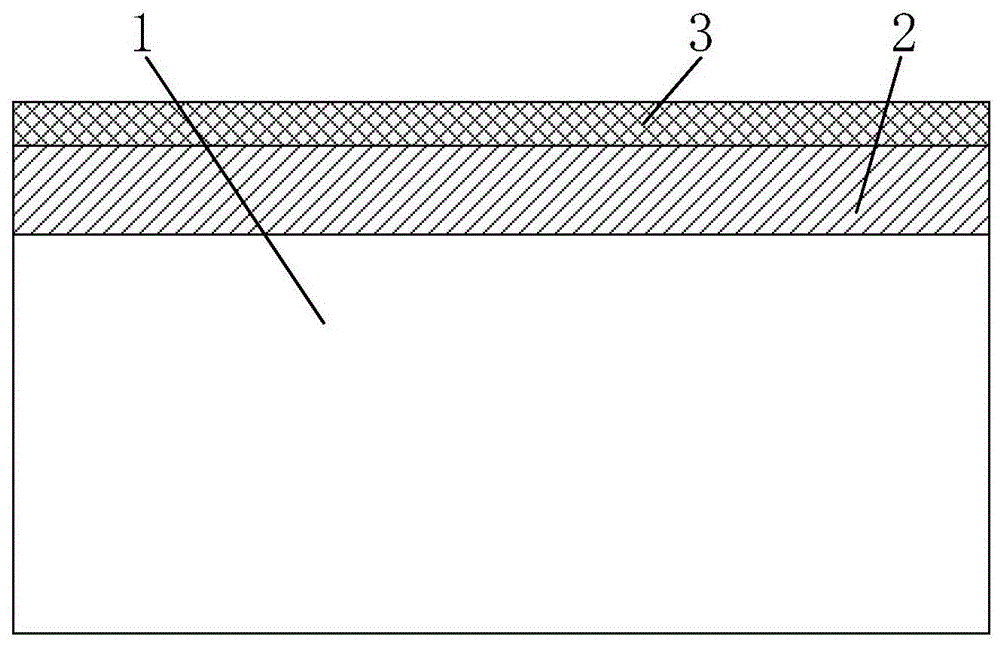
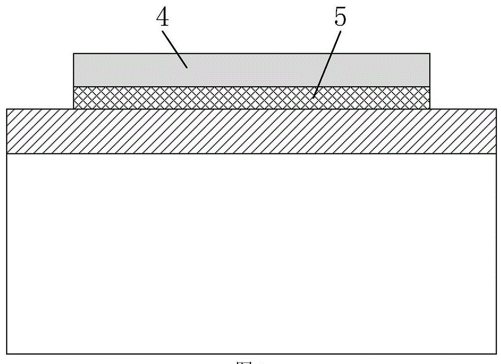
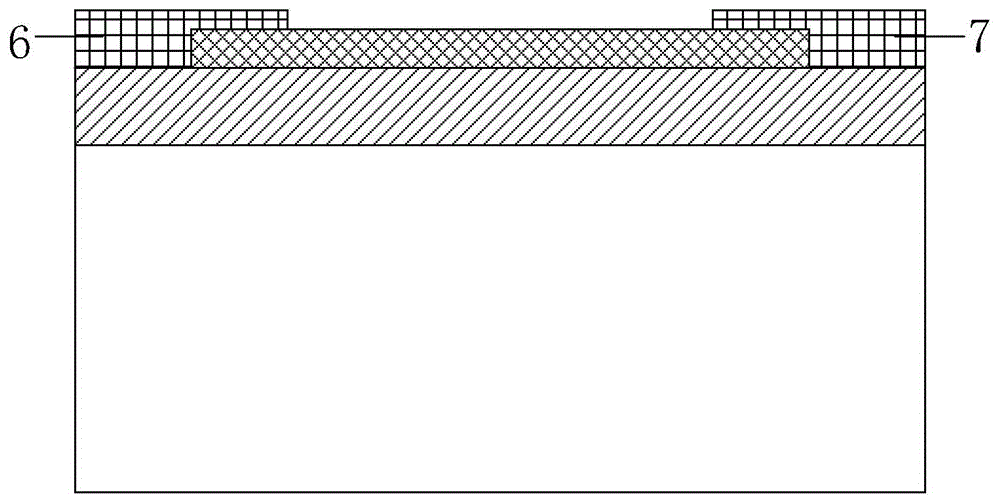
[0038] A specific example of the preparation method of the present invention includes Figure 1 to Figure 5 Process steps shown:

[0039] 1) The bottom gate electrode 1 is a low-resistance bulk silicon wafer with (100) crystal orientation, and the bottom gate dielectric layer 2 is grown on its surface by thermal oxidation, and the bottom gate dielectric layer is SiO 2 , The thickness is...


PUM


Abstract

A stepped gate-dielectric double-layer graphene field effect transistor comprises a bottom gate electrode, a bottom gate dielectric layer, a double-layer graphene active region, a metal source electrode, a metal drain electrode, a stepped top gate dielectric layer and a top gate electrode. The bottom gate dielectric layer is located on the bottom gate electrode, the double-layer graphene active region is located on the bottom gate dielectric layer, the metal source electrode and the metal drain electrode are located at two ends of the double-layer graphene active region respectively and cover the bottom gate dielectric layer and part of the double-layer graphene active region at the same time, the stepped top gate dielectric layer covers the metal source electrode, the metal drain electrode and graphene between the two electrodes, the top gate electrode only covers the top of the stepped top gate dielectric layer partially, and the distance between the top gate electrode and the edge of the metal source electrode is equal to that between the top gate electrode and the edge of the metal drain electrode. By introduction of the stepped top gate dielectric layer, a tunneling window between a source region and a gate-controlled trench under an off state is reduced effectively, so that small off-state current is obtained, and on-off ratio of a device is increased.

Description

Technical field [0001] The invention belongs to the technical field of nanoelectronics, and specifically relates to a step-gate dielectric double-layer graphene field effect transistor and a preparation method thereof. Background technique [0002] Graphene has become a research hotspot in nanoelectronics due to its excellent electrical properties. The ultra-thin channel and extremely high carrier mobility make it an ideal channel material for field effect transistors. However, to realize the application of graphene logic devices, opening the band gap to achieve a higher switching ratio is one of the main challenges. In response to this challenge, some solutions have been proposed. Among them, graphene nanoribbons (GNR) and double-layer graphene are considered to be the most promising solutions. Although GNR uses the quantum confinement effect to obtain a larger band gap, its application is restricted by reliable patterning technology. In addition, edge effects can cause degra...

Claims


Application Information

Patent Timeline
Patent Type & Authority Patents(China)
IPC IPC(8): H01L29/78H01L29/423H01L29/51H01L21/336
CPCH01L29/42368H01L29/42376H01L29/495H01L29/66477H01L29/78
Inventor 黄如王佳鑫黄芊芊吴春蕾朱昊赵阳
Owner PEKING UNIV
Why Eureka
Try Eureka