An anti-staggered layer heterojunction resonant tunneling field effect transistor and its preparation method

A field-effect transistor and resonant tunneling technology, which is applied in the field of field-effect transistor logic devices, can solve problems such as failure to meet system integration application requirements, low on-state current, and low band-band tunneling efficiency, and achieve suppression of device off-state current, The effect of increasing the on-state current and reducing the production cost

Active Publication Date: 2017-02-15
PEKING UNIV
View PDF4 Cites 0 Cited by
  • Summary
  • Abstract
  • Description
  • Claims
  • Application Information

AI Technical Summary

Problems solved by technology

[0003] However, due to the low efficiency of semiconductor band-band tunneling, the on-state current of TFET is lower than that of existing MOSFETs, which cannot meet the requirements of system integration applications.

Method used


Image

  • An anti-staggered layer heterojunction resonant tunneling field effect transistor and its preparation method
  • An anti-staggered layer heterojunction resonant tunneling field effect transistor and its preparation method
  • An anti-staggered layer heterojunction resonant tunneling field effect transistor and its preparation method

Examples


Embodiment Construction

[0048] The present invention will be further described through specific embodiments below in conjunction with the accompanying drawings.

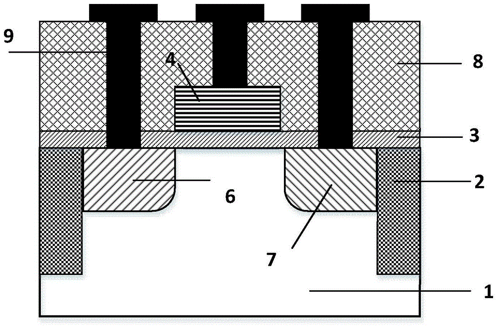
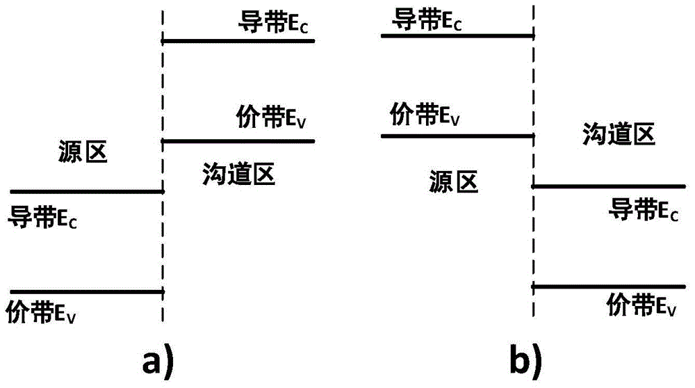
[0049] The anti-staggered layer type heterojunction resonant tunneling field effect transistor provided by the present invention has a structure such as figure 1 As shown, it includes a tunneling source region 6, a channel region 1, a drain region 7 and a control gate 4 located above the channel region 1, wherein the energy of the heterogeneous tunneling junction between the tunneling source region 6 and the channel region 1 The band structure is an anti-staggered layered heterojunction, such as Picture 1-1 , where: a) is the energy band structure of the N-type anti-staggered layer type heterojunction resonant tunneling transistor; b) is the P-type anti-staggered layer type heterojunction resonant tunneling transistor Tunneling junction anti-staggered layered energy band structure;.

[0050] The aforementioned anti-staggered layer hetero...


PUM


Abstract

The invention discloses an anti-staggered-layer heterojunction resonance tunneling field-effect transistor (TFET) and a preparation method thereof. The TFET comprises a tunneling source region, a channel region, a drain region and a control grid located above the channel region, wherein an electronic band structure of a heterogeneous tunneling junction of the tunneling source region and an electronic band structure of a heterogeneous tunneling junction of the channel region are respectively an anti-staggered-layer heterojunction. If the TFET is an N type device, the bottom of a conduction band of the tunneling source region is located below the valence band top of the channel region at the juncture surface of the heterogeneous tunneling junction of the tunneling source region and the heterogeneous tunneling junction of the channel region; if the TFET is a P type device, the valence band top of the tunneling source region is located above the bottom of a conduction band of the channel region. Thus, on-state currents of the TFET can be remarkably increased; meanwhile, off-state currents of the device are effectively suppressed, and a steep subthreshold slope is maintained. According to the preparation method of the TFET, a low-power dissipation integrated circuit formed by TFETs is prepared by effectively using a standard process, production cost is greatly reduced, and the process is simple.

Description

technical field [0001] The invention belongs to the field of CMOS ultra large scale integrated circuit (ULSI) field effect transistor logic devices, and specifically relates to an anti-staggered layer type heterojunction resonant tunneling field effect transistor and a preparation method thereof. Background technique [0002] Since the birth of integrated circuits, microelectronics integration technology has been developing continuously in accordance with "Moore's Law", and the size of semiconductor devices has been continuously reduced. As semiconductor devices enter the deep submicron range, existing MOSFET devices are limited by the conduction mechanism of self-diffusion drift, and the subthreshold slope is limited by the thermoelectric potential kT / q, which cannot be reduced synchronously with the reduction of device size. As a result, the reduction of leakage current of MOSFET devices cannot meet the requirements of device size reduction, the energy consumption of the e...

Claims


Application Information

Patent Timeline
Patent Type & Authority Patents(China)
IPC IPC(8): H01L29/78H01L29/41H01L21/336
CPCH01L29/66356H01L29/7391
Inventor 黄如吴春蕾黄芊芊王佳鑫王阳元
Owner PEKING UNIV
Why Eureka
Try Eureka