Semiconductor device and manufacturing method thereof

A manufacturing method and semiconductor technology, applied in the fields of semiconductor/solid-state device manufacturing, semiconductor devices, semiconductor/solid-state device components, etc., can solve problems such as increased cost, difficulty in mass production, and long time.

Active Publication Date: 2014-12-24
SONY CORP
View PDF7 Cites 6 Cited by
  • Summary
  • Abstract
  • Description
  • Claims
  • Application Information

AI Technical Summary

Problems solved by technology

[0009] However, the oxidation treatment in this process takes a long time (24 hours), so it is difficult to mass-produce and the cost will inevitably increase

Method used


Image

  • Semiconductor device and manufacturing method thereof
  • Semiconductor device and manufacturing method thereof
  • Semiconductor device and manufacturing method thereof

Examples


Embodiment Construction

[0045] Hereinafter, embodiments according to the present invention will be described.

[0046] Instructions are given in the following manner.

[0047] 1. Semiconductor device and manufacturing method of the embodiment

[0048] 1-1. Structure of semiconductor device

[0049] 1-2. Manufacturing method as the aforementioned example

[0050] 1-3. Problems in the preceding examples

[0051] 1-4. Manufacturing method of the example

[0052] 1-5. Outline of Embodiments

[0053] 2. Modification

[0054] 3. The present invention

[0055] 1. Semiconductor and manufacturing method of the embodiment

[0056] 1-1. Structure of semiconductor device

[0057] Hereinafter, embodiments according to the present invention will be described with reference to the drawings.

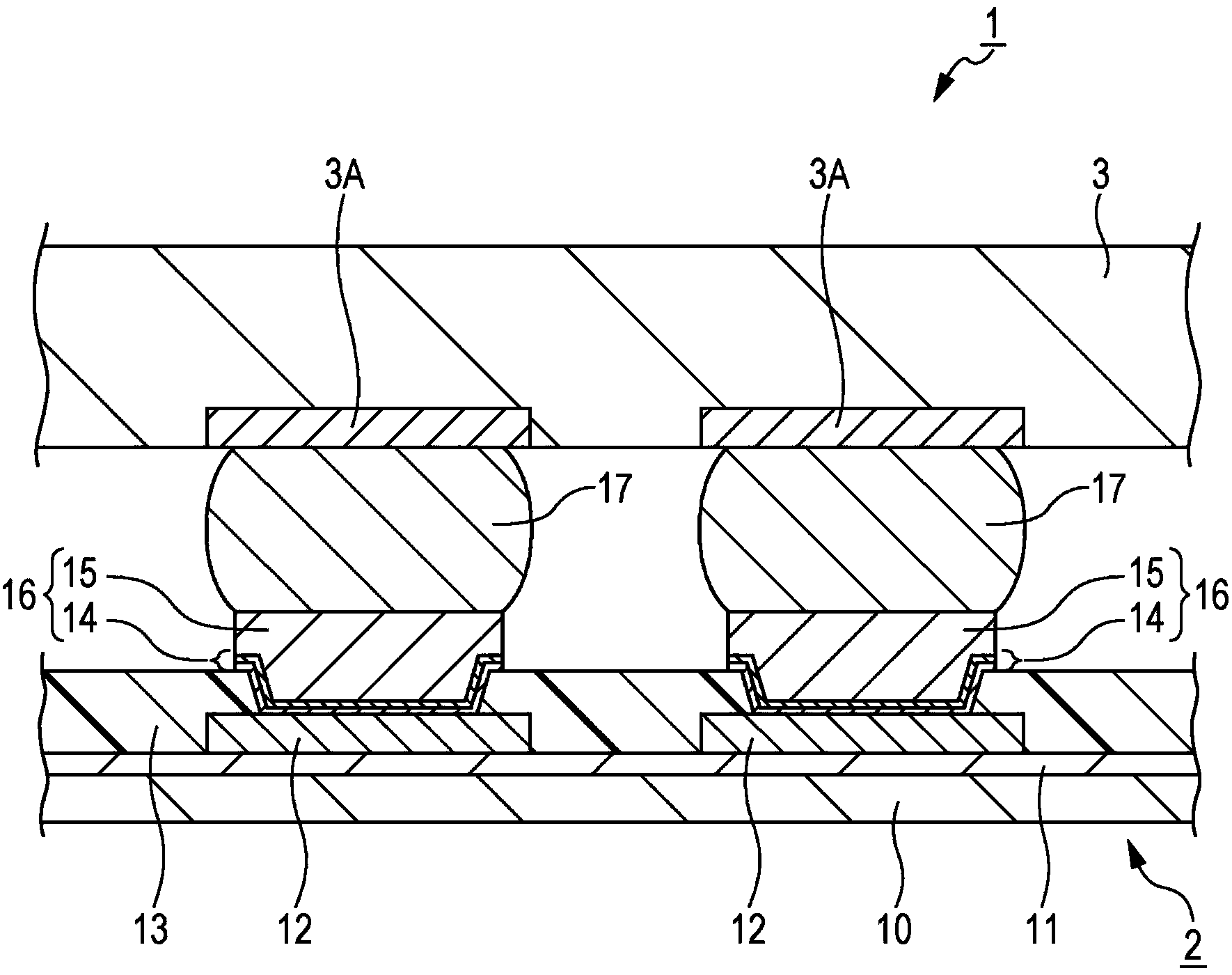
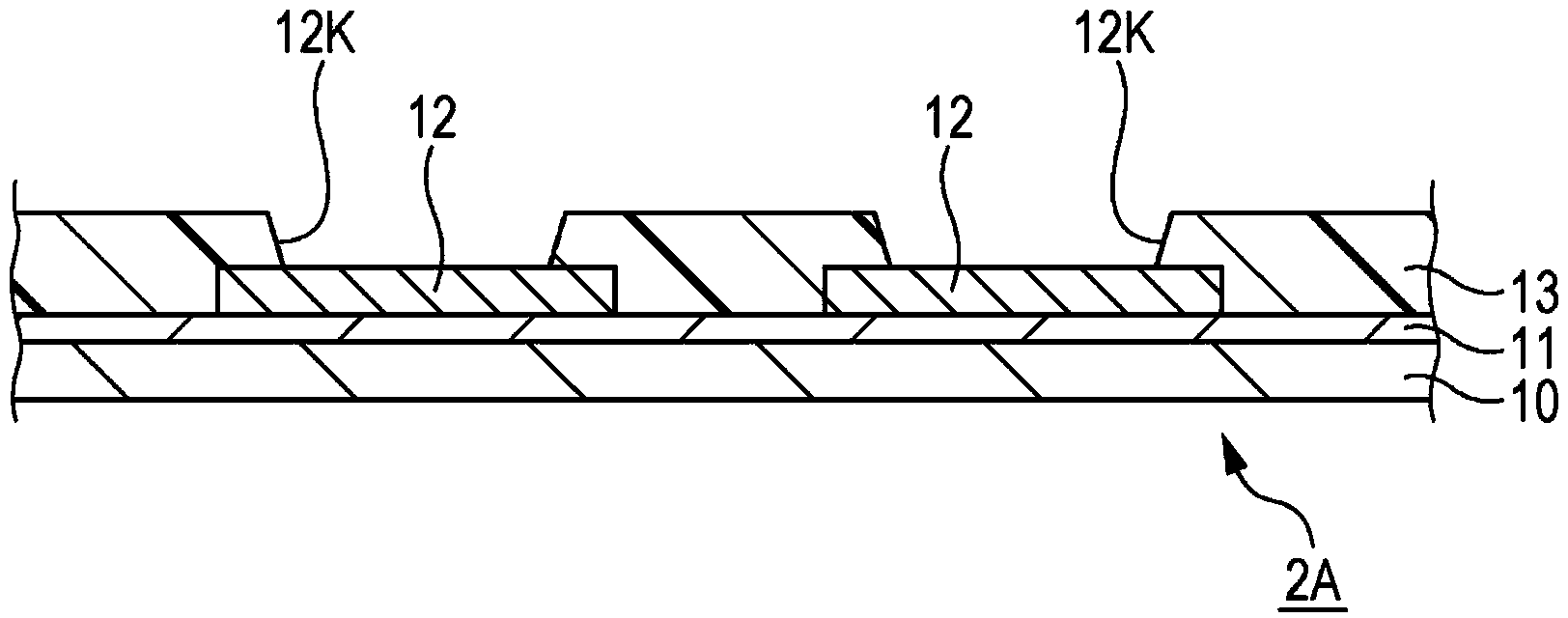
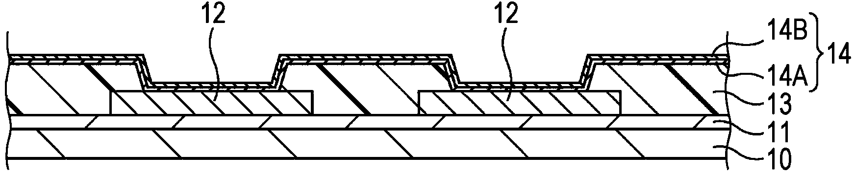
[0058] figure 1 is a schematic cross-sectional view of the semiconductor device 1 according to the embodiment.

[0059] First, as a premise, the semiconductor device 1 according to the embodiment is configured to ha...


PUM

PropertyMeasurementUnit
distanceaaaaaaaaaa
lengthaaaaaaaaaa
lengthaaaaaaaaaa

Abstract

The invention relates to a semiconductor device and a manufacturing method thereof. The semiconductor device includes a first semiconductor electronic component which includes a pad electrode, a solder bump, and a metal layer between a pad and solder that is configured to have an underlying metal layer formed between the pad electrode and the solder bump and connected to the pad electrode, and a main metal layer formed on the underlying metal layer, and in which the main metal layer has an eave portion at an outer edge portion thereof. Accordingly, the invention prevents the reduction in the reliability of electrical connection and mechanical connection between the semiconductor electronic components while suppressing a decrease in the mass production rate and an increase in the cost.

Description

technical field [0001] The present invention relates to a semiconductor device and a manufacturing method thereof, and more particularly to the technical field of a semiconductor device having a predetermined metal layer disposed between a pad electrode and a solder bump. Background technique [0002] For example, with a known flip chip method or the like, an IC chip (semiconductor chip) is bonded (mounted) to a mounting substrate including a semiconductor substrate through solder bumps. In a semiconductor device in which a semiconductor chip is mounted on a mounting substrate by solder bumps, an under-bump metal (hereinafter, referred to as "UBM") is arranged between a pad electrode and a solder bump (for example, refer to Japanese Unexamined Examined Patent Application 2008-28112 and Japanese Unexamined Patent Application 2012-80043). The UBM is configured to improve the bond adhesion between the pad electrode (eg, Al-based material) and the solder bump. [0003] For exa...

Claims


Application Information

Patent Timeline
Patent Type & Authority Applications(China)
IPC IPC(8): H01L23/488H01L21/60
CPCH01L2224/1146H01L2224/0558H01L24/03H01L24/05H01L2224/0345H01L2224/0346H01L2224/0347H01L2224/05541H01L2224/05557H01L2224/05647H01L2224/11462H01L2224/1181H01L2224/11849H01L2224/11903H01L2224/13007H01L2224/13018H01L2224/13082H01L2224/94H01L2924/3651H01L2224/03912H01L2224/13006H01L2224/11472H01L2224/11009H01L2224/05572H01L2224/03009H01L2224/0401H01L2224/05009H01L2224/05022H01L2224/05124H01L2224/05147H01L2224/05166H01L2224/1134H01L2224/0361H01L24/11H01L24/13H01L2924/00014H01L2924/00012H01L2924/207H01L2224/03H01L2224/11
Inventor 松本一治大鸟居英
Owner SONY CORP
Why Eureka
Try Eureka