Sidelobe Compression Method of Scanning Beam Based on Optical Waveguide Array Electro-optic Scanner

An electro-optic scanner and scanning beam technology, applied in the laser field, can solve problems such as unequal pitch design, infeasibility, large array element pitch design, etc., to achieve the effect of improving quality and avoiding processing technology

Active Publication Date: 2017-04-12
XIDIAN UNIV
View PDF1 Cites 0 Cited by
  • Summary
  • Abstract
  • Description
  • Claims
  • Application Information

AI Technical Summary

Problems solved by technology

Under the condition of flat end surface, this patent studies the side lobe compression of optical phased array by setting the irregular distribution of the array element spacing of the electro-optic scanner. However, in practical applications, the array element spacing of the optical waveguide array electro-optic scanner is determined by It is controlled by changing the cladding thickness of the optical waveguide. The above method will result in a large and unequal design of the array element spacing, which will cause great difficulties in the processing of the optical waveguide.
Therefore, for the optical waveguide array electro-optic scanner, it is not practical to compress the side lobes by setting the irregular distribution of the electro-optic scanner element spacing

Method used


Image

  • Sidelobe Compression Method of Scanning Beam Based on Optical Waveguide Array Electro-optic Scanner
  • Sidelobe Compression Method of Scanning Beam Based on Optical Waveguide Array Electro-optic Scanner
  • Sidelobe Compression Method of Scanning Beam Based on Optical Waveguide Array Electro-optic Scanner

Examples


Embodiment Construction

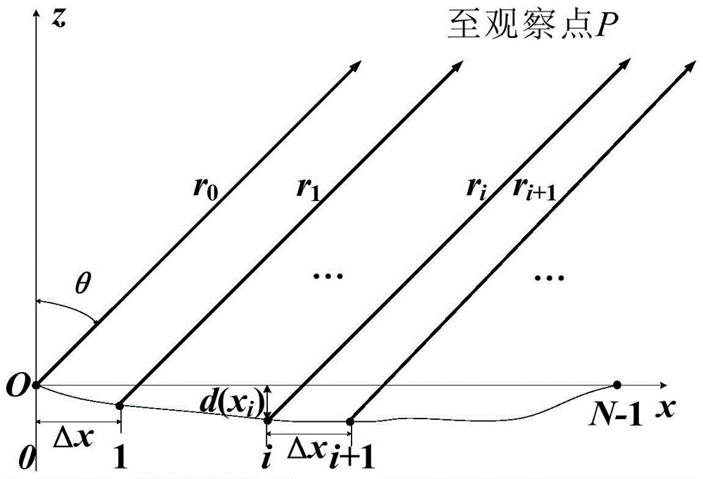
[0023] 1. Technical principles

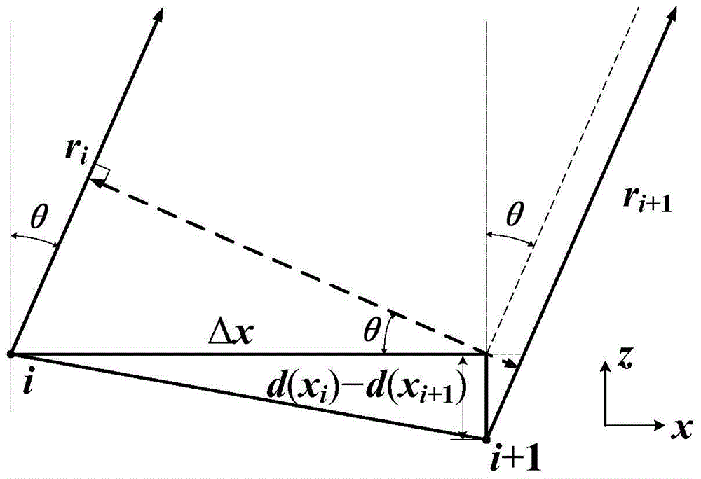
[0024] For an optical waveguide array with an uneven end face, the spatial diffraction geometric model is as follows figure 1 As shown, the output surface composed of N array elements is an arbitrary non-flat surface, and the end surface function d(x i ), defined as the position that deviates from the x-axis along the z-axis direction based on the x-axis. For a point P in the far field, its deflection angle relative to the z-axis direction is θ, and the optical field intensity E of the wavelength λ emitted by the i-th waveguide layer i (θ) is

[0025]

[0026] where A i is the optical field amplitude of the i-th array element, is the phase of the beam after passing through the waveguide, r i is the distance from the i-th array element to point P, f i (θ) is the tilt factor, θ is r i Angle with the z-axis.

[0027] The total optical field at point P is regarded as the total optical field superposition of all N array elements to point...


PUM

PropertyMeasurementUnit
thicknessaaaaaaaaaa

Abstract

The invention discloses a scanning beam side lobe compression method based on an optical waveguide array electro-optic scanner end face and solves the problem that an existing method is complex in the processing process. The method includes 1, setting parameters of an optical waveguide array electro-optic scanner, setting the end face as a paraboloid, and utilizing the end face to destroy the coherence of beams of array elements in the side lobe direction; 2, calculating the spatial distance of each optical waveguide array element to the far field; 3, calculating the spatial phase delay of each optical waveguide array element, setting the additional phase of each optical waveguide array element at the certain scanning angle according to the spatial phase delay so as to compensate the phase of each array element on the direction of scanning a main lobe, guaranteeing the main lobe being not weakened, and compressing the scanning beam side lobe; 4, calculating the light intensity distribution of the far field. The method is simple in processing process, the scanning beam side lobe can be compressed effectively, the scanning beam quality can be improved, and the method can be applied to laser radars, laser guidance and laser display.

Description

technical field [0001] The invention relates to the technical field of lasers, in particular to an optical scanning light beam edge lobe compression method, which can be used in laser radar, laser guidance and laser display. Background technique [0002] With the development of laser radar, laser guidance, and laser display technology, higher requirements are put forward for the characteristics of laser scanning. There are many technical solutions for laser scanning, such as optical mechanical scanning, electro-optical scanning, acousto-optic scanning, control technology, etc. [0003] Optical-mechanical scanning has been widely used in many systems such as infrared imaging, especially the micro-electro-mechanical scanning technology developed in recent years, which makes this technology more widely used. The advantages of optical-mechanical scanning are large scanning range and low optical loss, but due to the existence of inertial devices, complex and precise structure, e...

Claims


Application Information

Patent Timeline
Patent Type & Authority Patents(China)
IPC IPC(8): G02F1/29
CPCG02F1/292
Inventor 孙艳玲聂光鲁振中马琳石顺祥刘继芳韩香娥
Owner XIDIAN UNIV
Why Eureka
Try Eureka