Method for driving liquid crystal display panel

A driving signal, first-time technology, applied in static indicators, nonlinear optics, optics, etc., can solve problems such as uneven brightness and darkness of liquid crystal display panels, achieve uniform brightness and darkness, and eliminate bright and dark lines.

Inactive Publication Date: 2015-01-28
TCL CHINA STAR OPTOELECTRONICS TECH CO LTD
View PDF9 Cites 48 Cited by
  • Summary
  • Abstract
  • Description
  • Claims
  • Application Information

AI Technical Summary

Problems solved by technology

[0007] The technical problem to be solved by the present invention is to overcome the defect that the brightness and darkness of the liquid crystal display panel in the prior art are not uniform in space.

Method used


Image

  • Method for driving liquid crystal display panel
  • Method for driving liquid crystal display panel
  • Method for driving liquid crystal display panel

Examples


Embodiment 1

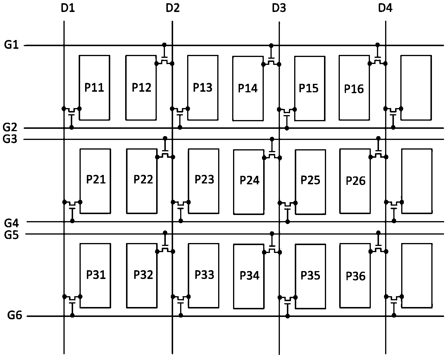
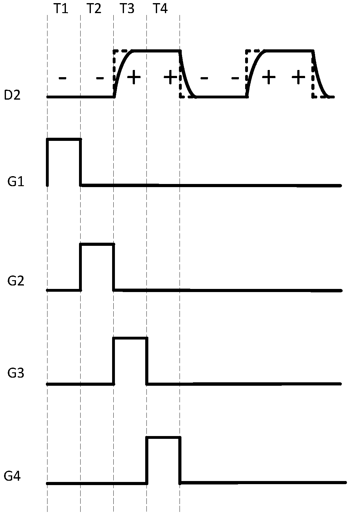
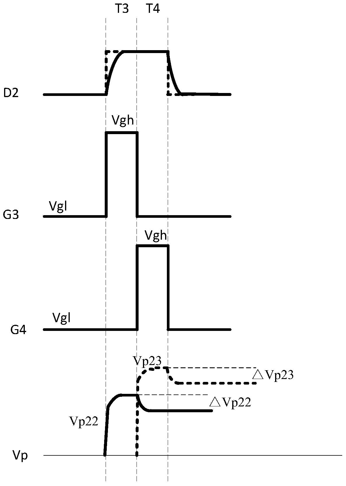
[0034] figure 1 It is a schematic structural diagram of a half source driving HSD (Half Source Driving) liquid crystal display panel of this embodiment. Such as figure 1 As shown, the display panel includes a plurality of data lines (data lines D1, D2, D3, D4 as shown in the figure) and a plurality of scanning lines (scanning lines G1, G2, G3, G4 as shown in the figure) ) a pixel array formed by an orthogonal arrangement, and a plurality of sub-pixels P11 to P36 arranged in the array. For the sake of brevity, it is defined here that the sub-pixel Pxy is disposed in the xth row and the yth column. For example, the sub-pixel P12 is arranged in the first row, the second column, and so on.

[0035] The sub-pixel P12 is connected to the scan line G1 and the data line D2, and the sub-pixel P13 is connected to the scan line G2 and the data line D2. P12 and P13 are respectively arranged on two sides of the data line D2. Similarly, the sub-pixel P22 is connected to the scan line G...

Embodiment 2

[0056] Figure 5 It is a schematic structural diagram of a tri-gate (Tri-Gate) liquid crystal display panel in this embodiment. Such as Figure 5 As shown, the display panel includes a pixel array formed by orthogonal arrangement of multiple data lines (data lines D1-D6 shown in the figure) and multiple scan lines (scan lines G1-G6 shown in the figure), And a plurality of sub-pixels P11-P66 arranged in the array. Wherein, the red sub-pixel (R) P11 , the green sub-pixel (G) P21 and the blue sub-pixel (B) P31 form a pixel unit.

[0057] In the case of a resolution of n*m, the number of scanning lines of the tri-gate liquid crystal display panel is 3m, and the number of data lines is n, while the number of scanning lines of an ordinary display panel is m, and the data of data lines is 3n . In other words, compared with the common display panel, under the same resolution, the number of scan lines of the tri-gate liquid crystal display panel is increased by three times, while t...


PUM


Abstract

The invention discloses a method for driving a liquid crystal display panel. The method comprises the following steps: providing a first scanning signal within the first time quantum of a data wire driving a signal level to reversing, in order to open a first scanning wire; charging a first sub-pixel which is connected with the first scanning wire through the data wire; providing a second scanning signal to open at least one scanning wire; charging a second sub-pixel which is connected with the second scanning wire through the data wire, wherein the start voltage of the first scanning signal is more than the start voltage of the second scanning signal; the chamfer voltage of the first scanning signal is the same as the chamfer of the second scanning signal.

Description

technical field [0001] The invention relates to the field of display technology, in particular to a method for driving a liquid crystal display panel. Background technique [0002] With the development of liquid crystal display technology, most of the current liquid crystal displays have the advantages of low cost, low power consumption and high performance. The various components of the LCD panel are often integrated through precise design to ensure the best display effect while reducing cost and power consumption. [0003] In the thin film transistor-liquid crystal display (TFT-LCD) field, a large number of source driving circuits and gate driving circuits need to be arranged in the liquid crystal display panel to drive pixels vertically and horizontally. Compared with the source driver chip, the cost and power consumption of the gate driver chip are lower, so the number of data lines can be reduced by rationally designing the structure of the pixel array, thereby using f...

Claims


Application Information

Patent Timeline
Patent Type & Authority Applications(China)
IPC IPC(8): G02F1/133G09G3/36
CPCG09G3/3614G09G2320/0233G09G2230/00G09G3/3648G09G2300/0426G09G2310/067G09G2320/0219G09G2320/0223G02F1/136286G02F1/134345G02F1/134336G02F2201/123G09G3/3677G09G3/3688G09G2300/0452G09G2310/0251G09G2310/06G09G2330/021
Inventor 陈彩琴许哲豪
Owner TCL CHINA STAR OPTOELECTRONICS TECH CO LTD
Why Eureka
Try Eureka