Array substrate, manufacturing method of array substrate and display device

A technology for array substrates and display devices, which is applied in semiconductor/solid-state device manufacturing, electrical components, electric solid-state devices, etc., and can solve problems such as threshold voltage drift, affecting the uniformity of the display screen, and increasing power consumption of the display

Active Publication Date: 2015-01-28
BOE TECH GRP CO LTD
View PDF4 Cites 11 Cited by
  • Summary
  • Abstract
  • Description
  • Claims
  • Application Information

AI Technical Summary

Problems solved by technology

However, the active layer in the thin film transistor (Thin Film Transistor, TFT) on the AMOLED (Active Matrix Organic Light Emitting Diode, active matrix organic light emitting diode) substrate will experience a threshold voltage shift under the irradiation of these lights, affecting Improve the uniformity of the display screen and i...

Method used


Image

  • Array substrate, manufacturing method of array substrate and display device
  • Array substrate, manufacturing method of array substrate and display device
  • Array substrate, manufacturing method of array substrate and display device

Examples


Embodiment Construction

[0045] In order to make the purpose, technical solutions and advantages of the embodiments of the present invention clearer, the technical solutions in the embodiments of the present invention will be clearly and completely described below in conjunction with the drawings in the embodiments of the present invention. Obviously, the described embodiments It is a part of embodiments of the present invention, but not all embodiments. Based on the embodiments of the present invention, all other embodiments obtained by persons of ordinary skill in the art without creative efforts fall within the protection scope of the present invention.

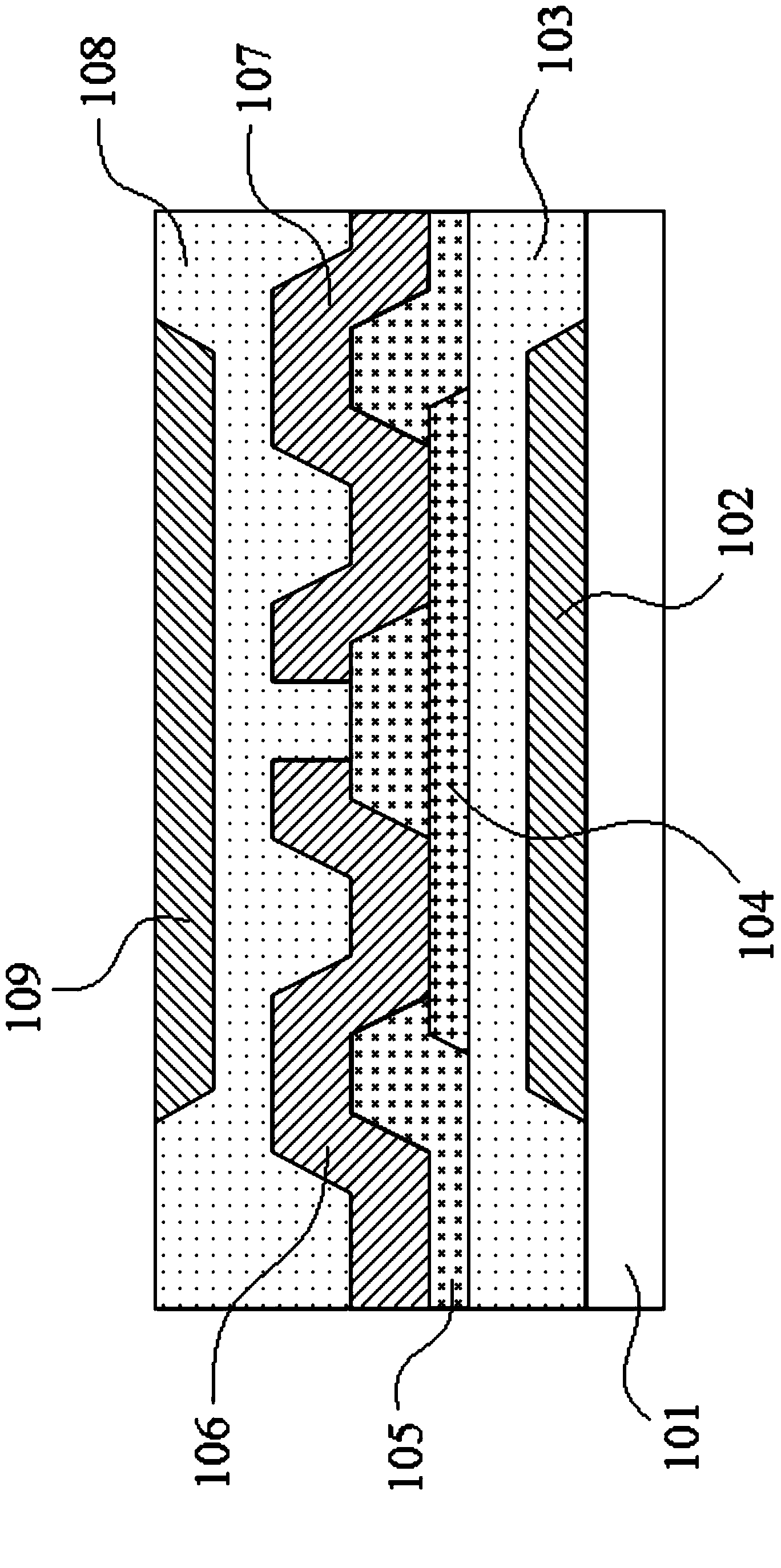
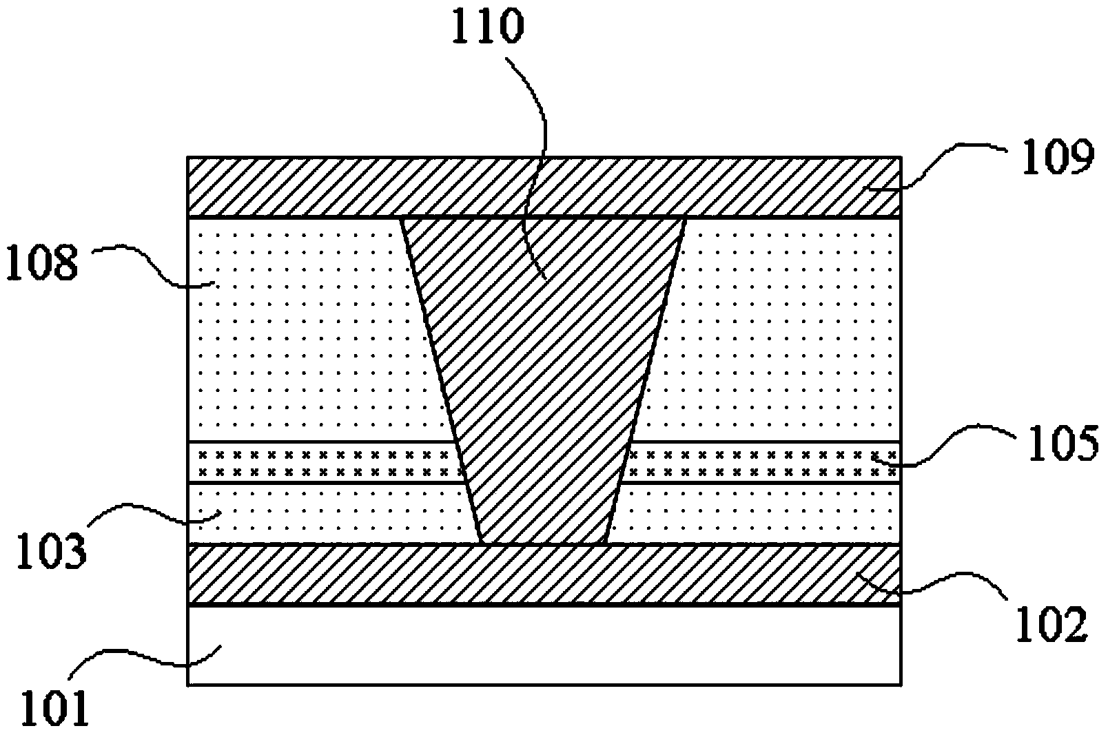
[0046] figure 1 It is a partial cross-sectional view of an array substrate in an embodiment of the present invention. see figure 1 , the array substrate includes:

[0047] The first gate metal layer 102 can specifically include the gate region of the thin film transistor TFT, the wiring of the scanning signal line and / or the high-level voltage ...


PUM


Abstract

The invention relates to the technical field of display, in particular to an array substrate, a manufacturing method of the array substrate and a display device. The array substrate comprises a first gate metal layer, a first gate insulating layer on the first gate metal layer, an active layer which is arranged on the first gate insulating layer and corresponds to the first gate metal layer, an etching barrier layer on the active layer, a source and drain metal layer comprising a source and a drain, a second gate insulating layer on the source and drain metal layer and a second gate metal layer on the second gate insulating layer, wherein the source and the drain are in contact with the two sides of the active layer respectively and are separated on the etching barrier layer. By means of the array substrate, the manufacturing method of the array substrate and the display device, the TFT characteristic can be optimized, the gate line resistance can be reduced, light irradiating the active layer can be shielded, IR Drop and TFT threshold voltage excursion and generation of the light leakage current of the active layer can be easily restrained, and the performance of the display device can be promoted.

Description

technical field [0001] The present invention relates to the field of display technology, in particular to an array substrate, a manufacturing method thereof, and a display device. Background technique [0002] In recent years, Organic Light Emitting Diode (OLED) has become a very popular emerging flat-panel display product at home and abroad, because OLED display has self-illumination, wide viewing angle, short response time, high luminous efficiency, wide color gamut, low It has the characteristics of working voltage, thin panel, large-size and flexible panel and simple manufacturing process, and it also has the potential to further develop to low cost. [0003] However, in large-scale display applications, since there is a certain resistance in the backplane power supply line, and the driving current of all pixels is provided by the unit power supply line ARVDD, the power supply voltage in the area close to the ARVDD power supply position in the backplane is relatively far...

Claims


Application Information

Patent Timeline
IPC IPC(8): H01L27/12H01L21/77H01L27/32
CPCH01L29/4908H01L29/78633H01L29/7869H01L27/1255H01L27/1248H01L27/124H01L27/127H01L29/78648H10K59/1213H10K59/126H01L27/1251H01L29/78645H01L29/78678H10K59/123H10K59/124H10K59/1201H01L21/77H01L27/12H01L27/1214
Inventor 盖翠丽宋丹娜张保侠
Owner BOE TECH GRP CO LTD
Why Eureka
Try Eureka