A high electron mobility transistor having high withstand voltage capability

A high electron mobility, transistor technology, applied in the direction of transistors, circuits, electrical components, etc., to achieve the effect of improving the withstand voltage

Pending Publication Date: 2021-03-05
GUANGDONG ZHINENG TECH CO LTD
View PDF0 Cites 1 Cited by
  • Summary
  • Abstract
  • Description
  • Claims
  • Application Information

AI Technical Summary

Problems solved by technology

However, the field plate structure usually uses metal materials, and there is still the problem of tip discharge, and there are still local electric field spikes

Method used


Image

  • A high electron mobility transistor having high withstand voltage capability
  • A high electron mobility transistor having high withstand voltage capability
  • A high electron mobility transistor having high withstand voltage capability

Examples


Embodiment Construction

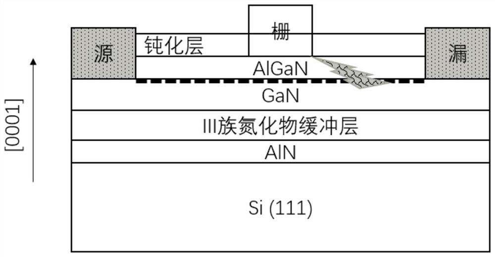
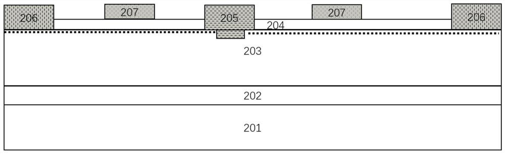
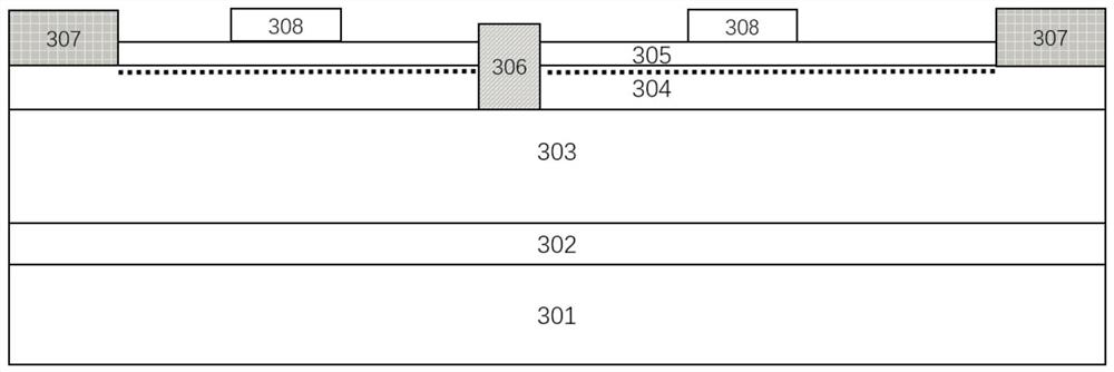
[0031] The technical solutions in the embodiments of the present application will be described below with reference to the drawings in the embodiments of the present application.

[0032] It should be noted that like numerals and letters denote similar items in the following figures, therefore, once an item is defined in one figure, it does not require further definition and explanation in subsequent figures. Meanwhile, in the description of the present application, the terms "first", "second" and the like are only used to distinguish descriptions, and cannot be understood as indicating or implying relative importance. "Up and down" and the like indicate a relative positional relationship, and do not mean that the two are directly adjacent to each other.

[0033] In the high electron mobility transistor of the present application, the doping concentration of strong doping generally refers to a doping concentration above 2E18 / cm3, and may even be as high as 5E19 / cm3 or higher. ...


PUM


Abstract

The invention relates to a semiconductor power device, in particular to a high-voltage-withstanding high-electron-mobility transistor (HEMT). The high-voltage-withstanding high-electron-mobility transistor comprises a gate electrode, a source electrode, a drain electrode, a barrier layer, a P-type nitride semiconductor layer and a substrate, the P-type nitride semiconductor layer is located between the barrier layer and the substrate, which is insufficient to significantly deplete the two-dimensional electron gas in the channel other than the gate stack, and the source electrode is in electrical contact with the P-type nitride semiconductor layer, and both the source electrode and the drain electrode are in electrical contact with the two-dimensional electron gas.

Description

technical field [0001] The present application relates to semiconductor power devices, in particular, to a high withstand voltage high electron mobility transistor (HEMT). Background technique [0002] Group III nitride semiconductor is an important new semiconductor material, mainly including AlN, GaN, InN and compounds of these materials such as AlGaN, InGaN, AlInGaN, etc. Due to the advantages of direct band gap, wide band gap, and high breakdown electric field strength, group III nitride semiconductors represented by GaN have broad application prospects in the fields of light-emitting devices, power electronics, and radio frequency devices. [0003] An important device type of III-nitride semiconductors is the high electron mobility transistor (HEMT), which has great promise in the field of power semiconductors. Due to the existence of spontaneous polarization and piezoelectric polarization effects, there is a strong polarized positive charge at the interface between Ga...

Claims


Application Information

Patent Timeline
Patent Type & Authority Applications(China)
IPC IPC(8): H01L29/778H01L29/207H01L29/10H01L21/335
CPCH01L29/66462H01L29/7787H01L29/207H01L29/1029H01L29/7786H01L29/41766H01L29/1075H01L29/1087H01L29/0603H01L29/2003H01L29/778H01L21/02645H01L29/66431H01L29/0847
Inventor 黎子兰
Owner GUANGDONG ZHINENG TECH CO LTD
Why Eureka
Try Eureka