GaN transistor device with high-linearity composite gate structure and preparation method thereof

A high linearity, transistor technology, applied in the field of microelectronics, can solve the problems of poor gate control ability, low current driving ability, poor performance, etc., and achieve the effect of reducing off-state leakage current, high current driving ability, and good switching characteristics

Active Publication Date: 2021-05-21
XIDIAN UNIV
View PDF7 Cites 1 Cited by
  • Summary
  • Abstract
  • Description
  • Claims
  • Application Information

AI Technical Summary

Problems solved by technology

[0004] At present, conventional multi-channel devices or nano-channel three-dimensional gate structure devices have poor gate control capability, low current drive capability, and poor linearity performance. Therefore, it is necessary to provide a large Current drive capability, improve the linear operating characteristics of the device, GaN transistor devices that meet the application requirements of GaN-based electronic devices in the field of communication, such as high linearity, high power density, high frequency and high bandwidth

Method used


Image

  • GaN transistor device with high-linearity composite gate structure and preparation method thereof
  • GaN transistor device with high-linearity composite gate structure and preparation method thereof
  • GaN transistor device with high-linearity composite gate structure and preparation method thereof

Examples


Embodiment 1

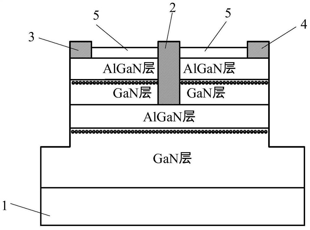
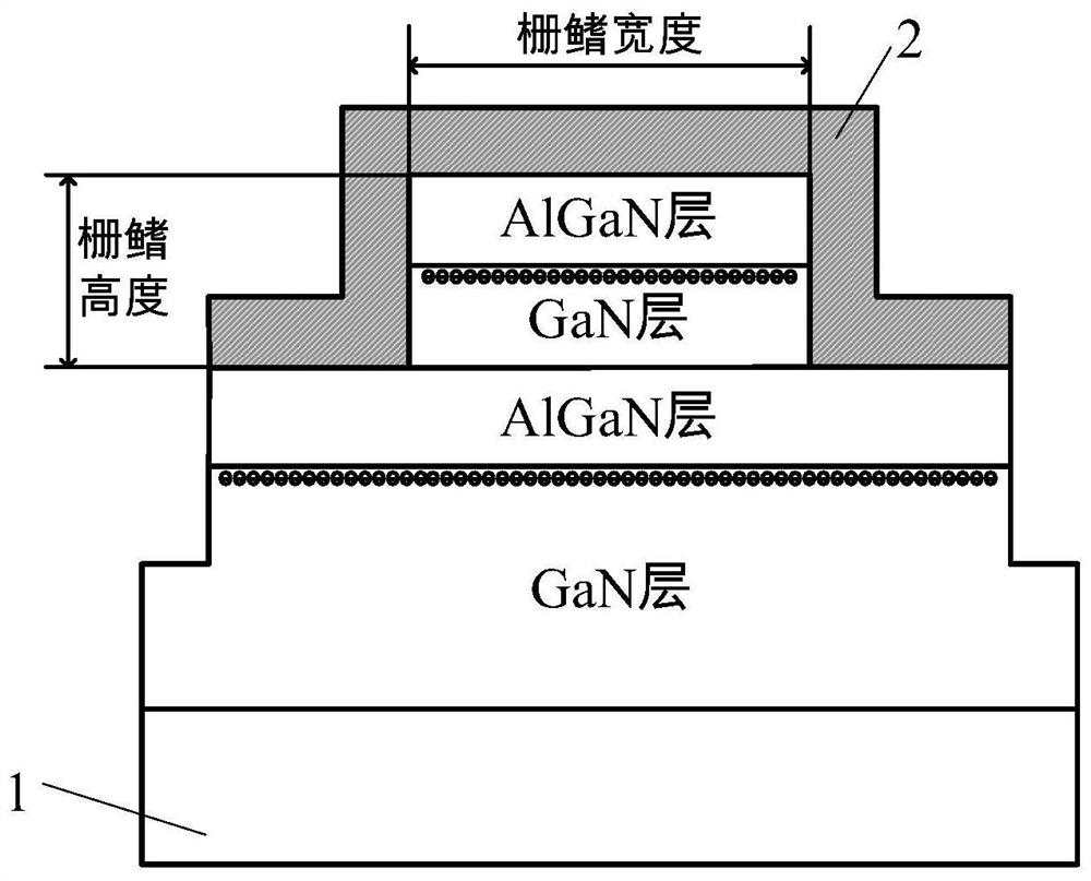
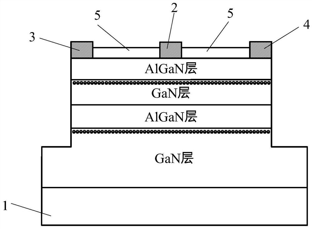
[0048] Please refer to Figure 1-Figure 3 , figure 1 It is a schematic cross-sectional view in the direction of the outer gate length of the gate fin of a GaN transistor device with a high linearity composite gate structure provided by an embodiment of the present invention; figure 2 It is a schematic cross-sectional view in the gate width direction of a GaN transistor device with a high linearity composite gate structure provided by an embodiment of the present invention; image 3 It is a schematic cross-sectional view of the inner gate length direction of the gate fin of a GaN transistor device with a high linearity composite gate structure provided by an embodiment of the present invention. As shown in the figure, the GaN transistor device with a high linearity composite gate structure in this embodiment includes:

[0049] substrate layer 1;

[0050] Several channel layers, several of which are sequentially stacked on the substrate layer 1;

[0051]The gate 2 is arrang...

Embodiment 2

[0065] In this embodiment, a GaN transistor device with a double channel layer and high linearity composite gate structure is taken as an example to illustrate its preparation method. See Figures 4a-4i , Figures 4a-4i It is a schematic process flow diagram of a GaN transistor device with a high linearity composite gate structure provided by an embodiment of the present invention. The preparation method includes the following steps:

[0066] Step 1: Select sapphire or SiC as the substrate layer 1, see Figure 4a ;

[0067] Step 2: On the sapphire substrate or SiC substrate layer 1, grow a GaN buffer layer and an AlGaN barrier layer to form an AlGaN / GaN heterojunction as a channel layer, wherein the thickness of the AlGaN layer is 15-25 nm, and the mole of A The score is 25-35%, see Figure 4b ;

[0068] Step 3: Repeat step 2 to form a double channel layer, see Figure 4c ;

[0069] Step 4: Provide active area mesa isolation on the dual channel layer, see Figure 4d ; ...

Embodiment 3

[0079] In this embodiment, taking different AlGaN barrier layer thicknesses and different Al compositions as examples, the specific process flow of the preparation method of the second embodiment is described in detail.

[0080] 1. A double channel layer with an AlGaN barrier layer thickness of 15nm, in which the Al component is 35%, the specific preparation steps are as follows:

[0081] Step 1. Epitaxial material growth

[0082] 1.1) On the SiC substrate, a GaN buffer layer is grown by MOCVD process;

[0083] 1.2) On the GaN buffer layer, grow a 15nm-thick AlGaN barrier layer, wherein the Al composition is 35%, and form a two-dimensional electron gas 2DEG at the contact position between the GaN buffer layer and the AlGaN barrier layer;

[0084] 1.3) growing a second layer of 10nm thick GaN buffer layer on the first layer of AlGaN barrier layer;

[0085] 1.4) A second 15nm-thick AlGaN barrier layer is grown on the second GaN buffer layer, wherein the Al composition is 35%, ...


PUM

PropertyMeasurementUnit
thicknessaaaaaaaaaa
widthaaaaaaaaaa
thicknessaaaaaaaaaa

Abstract

The invention relates to a GaN transistor device with a high-linearity composite gate structure and a preparation method of the GaN transistor device. The GaN transistor device comprises a substrate layer; a plurality of channel layers, wherein the plurality of channel layers are stacked on the substrate layer in sequence; grid electrodes arranged on the two sides and the tops of the channel layers and located in the middle of the GaN transistor device, wherein the grid electrodes are not arranged at the two sides of at least the channel layer on the bottommost layer; source electrodes arranged on the plurality of channel layers and positioned at a position close to one side of the GaN transistor device; and drain electrodes arranged on the plurality of channel layers and positioned at a position, close to the other side, of the GaN transistor device. The GaN transistor device provided by the invention has relatively high current driving capability, high linearity and low static power consumption.

Description

technical field [0001] The invention belongs to the technical field of microelectronics, and in particular relates to a GaN transistor device with a high linearity composite gate structure and a preparation method thereof. Background technique [0002] In recent years, the third-generation wide-bandgap semiconductors represented by SiC and GaN have been widely used due to their large bandgap, high breakdown electric field, high thermal conductivity, high saturation electron velocity and high concentration of 2DEG at the heterojunction interface. focus on. In theory, high electron mobility transistor HEMT, light-emitting diode LED, laser diode LD and other devices made of these materials have obvious superior characteristics than existing devices. [0003] Due to the high-concentration two-dimensional electron gas formed by the AlGaN / GaN heterojunction, GaN materials have obvious superior characteristics in terms of high current and high frequency compared with existing Si M...

Claims


Application Information

Patent Timeline
Patent Type & Authority Applications(China)
IPC IPC(8): H01L29/20H01L29/423H01L21/336H01L29/78
CPCH01L29/2003H01L29/42356H01L29/78H01L29/66477
Inventor 王冲李昂马晓华郑雪峰刘凯赵垚澎何云龙郝跃
Owner XIDIAN UNIV
Why Eureka
Try Eureka