Phase change memory device and fabrication method thereof

a memory device and phase change technology, applied in the field of memory devices, can solve the problems of affecting voltage drop, insufficient resistance of the bottom electrode 104/b> comprising tan, etc., and achieve the effect of increasing design flexibility and small parasitic resistan

Inactive Publication Date: 2009-02-05
IND TECH RES INST +5
View PDF2 Cites 35 Cited by
  • Summary
  • Abstract
  • Description
  • Claims
  • Application Information

AI Technical Summary

Benefits of technology

[0009]A detailed description is given in the following embodiments with reference to the accompanying drawings. These and other problems are generally solved or circumvented, and technical advantages are generally achieved, by the invention. Specif

Problems solved by technology

The phase change memory device 100, however, has higher parasitic resistance, thus affecting voltage

Method used


Image

  • Phase change memory device and fabrication method thereof
  • Phase change memory device and fabrication method thereof
  • Phase change memory device and fabrication method thereof

Examples


Embodiment Construction

[0017]The following description is of the contemplated mode of carrying out the invention. This description is made for the purpose of illustrating the general principles of the invention and should not be taken in a limiting sense. The scope of the invention is best determined by reference to the appended claims. Embodiments of the invention, which provide a phase change memory device, will be described in greater detail by referring to the drawings that accompany the invention. It is noted that in the accompanying drawings, like and / or corresponding elements are referred to by like reference numerals.

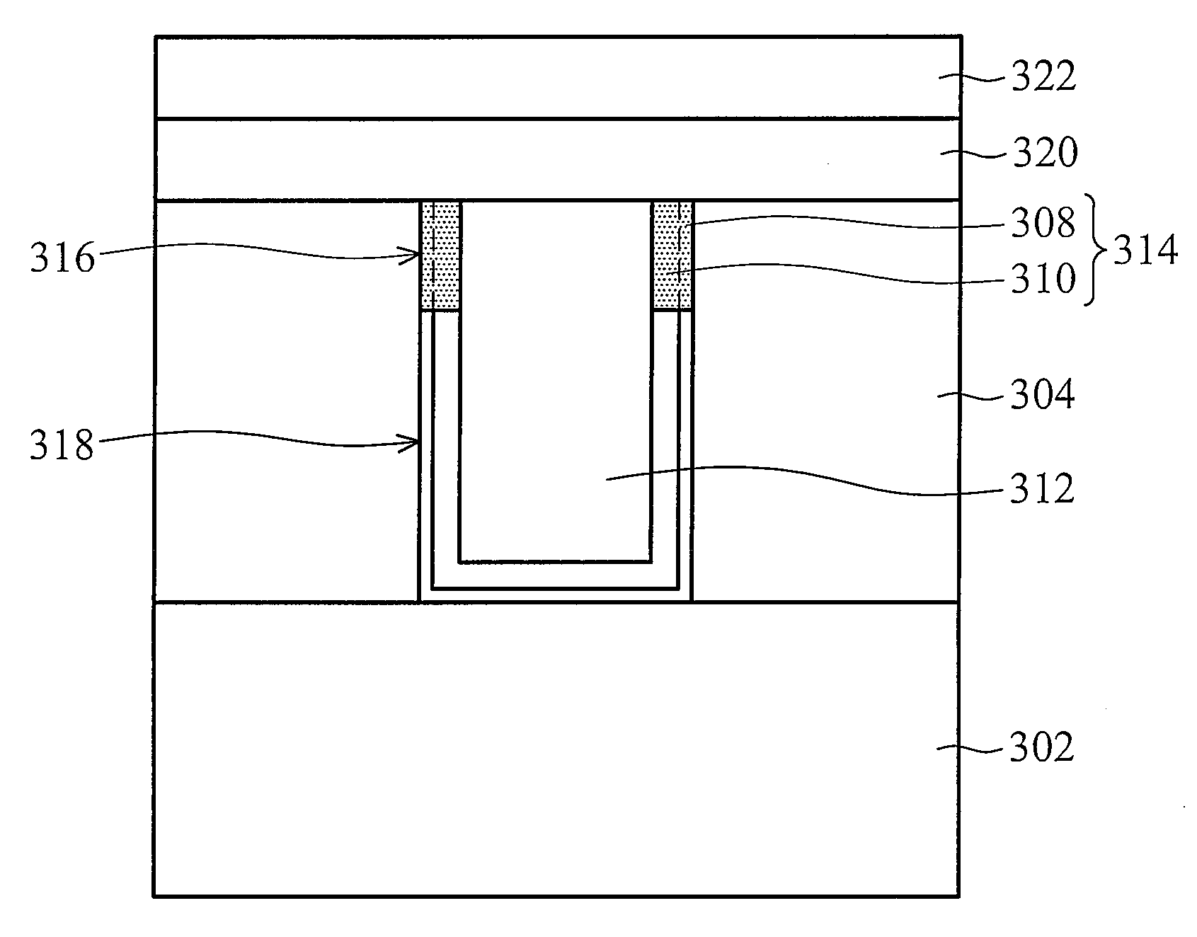
[0018]FIGS. 3A˜3G show intermediate cross sections of a phase change memory device of an embodiment of the invention. Referring to FIG. 3A, a semiconductor substrate 302, such as silicon, is provided. The substrate 302 is shown as a plane substrate for simplification, but the substrate 302 can comprise semiconductor devices, such as MOS transistors, resistors and / or logic devices. In ...


PUM


Abstract

A phase change memory device is disclosed. A first dielectric layer having a sidewall is provided. A bottom electrode is adjacent to the sidewall of the first dielectric layer, wherein the bottom electrode comprises a seed layer and a conductive layer. A second dielectric layer is adjacent to a side of the bottom electrode opposite the sidewall of the first dielectric layer. A top electrode couples the bottom electrode through a phase change layer.

Description

BACKGROUND OF THE INVENTION[0001]1. Field of the Invention[0002]The invention relates to a memory device and more particularly, relates to a phase change memory device and fabrication method thereof.[0003]2. Description of the Related Art[0004]Phase change memory devices have many advantages, such as faster speeds, lower power consumption, large capacity, greater endurance, better processing integrity and lower cost. Phase change memory devices can thus be used as stand-alone or embedded memory devices with high degree of integrity. Due to the described advantages and others, phase change memory device may substitute in place of volatile memory devices, such as SRAM and DRAM, or non-volatile memory devices, such as flash memory devices for respective applications.[0005]Phase change memory devices write, read or erase according to different resistances of a phase change material between a crystal state and a non-crystal state. For example, a relatively high current and short pulse, s...

Claims


Application Information

Patent Timeline
IPC IPC(8): H01L29/06H01L21/425
CPCH01L45/06H01L45/16H01L45/126H01L45/1233H10N70/8413H10N70/231H10N70/011H10N70/826
Inventor HSIAO, TSAI-CHU
Owner IND TECH RES INST
Why Eureka
Try Eureka