Fiber optic module

a fiber optic module and fiber optic technology, applied in the field of fiber optic modules, can solve the problems of limiting the design flexibility of mother boards of system manufacturers, affecting the requiring the inevitable large size of the entire unit, so as to achieve high design flexibility of mother boards, low cost, and compact size

Inactive Publication Date: 2008-03-11
II VI DELAWARE INC
View PDF537 Cites 51 Cited by
  • Summary
  • Abstract
  • Description
  • Claims
  • Application Information

AI Technical Summary

Benefits of technology

[0015]It is accordingly an object of the present invention to provide a fiber optic module which can solve the above problems in the prior art and can be made compact in size, high in the design flexibility of mother board, low in cost and high in reliability.

Problems solved by technology

However, the above prior art has had several problems which follow.
1) The electric signals are transferred on a parallel data basis, and then even though each of parallel signals consists of, e.g., 8 bits, the number of signal lines transferring the parallel signals as well as other signals becomes as many as 50, which requires the large size of connectors and semiconductor ICs for serial / parallel conversion, which results in that the size of the entire unit must be inevitably made large.
Further, not only the large size of this unit per se goes against a recent tendency of the rapid downsizing movement of host computer but this also largely limits the design flexibility of mother board for system manufacturers.
This requires a large hole as an opening for fixation in the mother board, whereby the design flexibility of the mother board by the system manufacturer is largely limited.
Further, since the prior art has such a structure that a load caused by the force derived by mounting and dismounting of the optical fiber is applied to the J-letter shaped clip 9 and the lead (not shown) of the connector 6, this causes a breakage of the J-letter shaped resin-clip 9 made from resin or a poor connection of the connector lead, with the result of reduction in the reliability of the fiber optic module.
Furthermore, for the purpose of avoiding any stress applied to the leads of the LD modules 1 and PD modules 2, the accuracy of each of the parts must be increased and thus parts management (such as parts acceptance inspection) becomes necessary, which make it difficult to obtain a low-cost fiber optic module.
The necessity of these works hinders realization of a low-cost fiber optic module.
Further, the holding method shown in FIG. 19 requires a sufficient length of the circuit board 3 itself and a sufficient circuit-board holding length L, which hinders realization of a miniaturized fiber optic module.
5) Since most area of the circuit board is in its exposed state, when a worker handles the prior art fiber optic module or a user mounts the prior art fiber optic module onto the mother board, the prior art fiber optic module is susceptible to electrostatic destruction, which leads to poor reliability and costliness of the fiber optic module.
6) During a long-term storage, dust or foreign matter invades into the LD and PD modules into which optical fibers are to plug, which causes improper or poor connection between the optical fiber and the module, thus resulting in remarkable reduction in the reliability of the fiber optic module.

Method used


Image

  • Fiber optic module
  • Fiber optic module
  • Fiber optic module

Examples


Embodiment Construction

[0041]The present invention will be explained with reference to the accompanying drawings, in which parts having the same reference numerals represent identical parts.

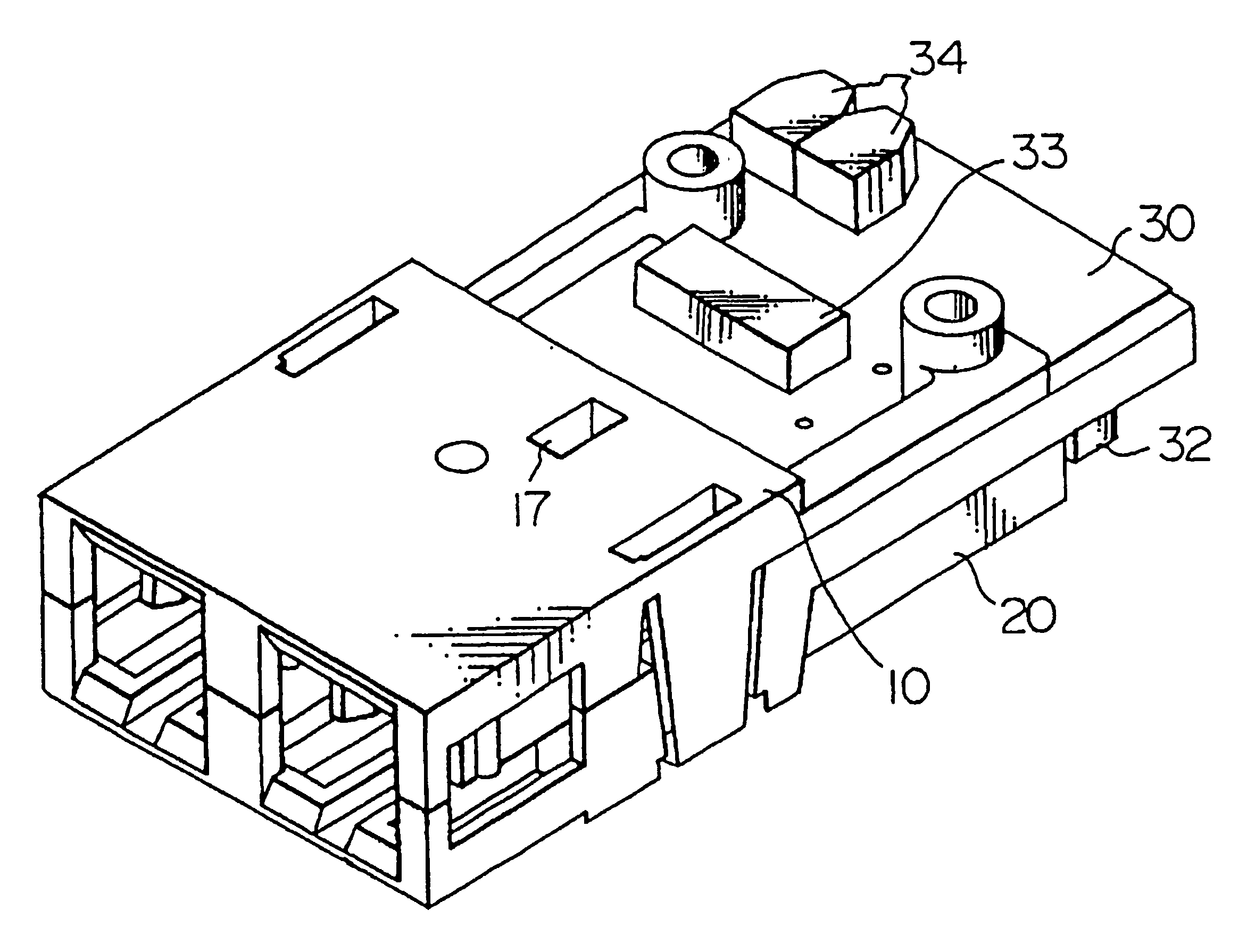
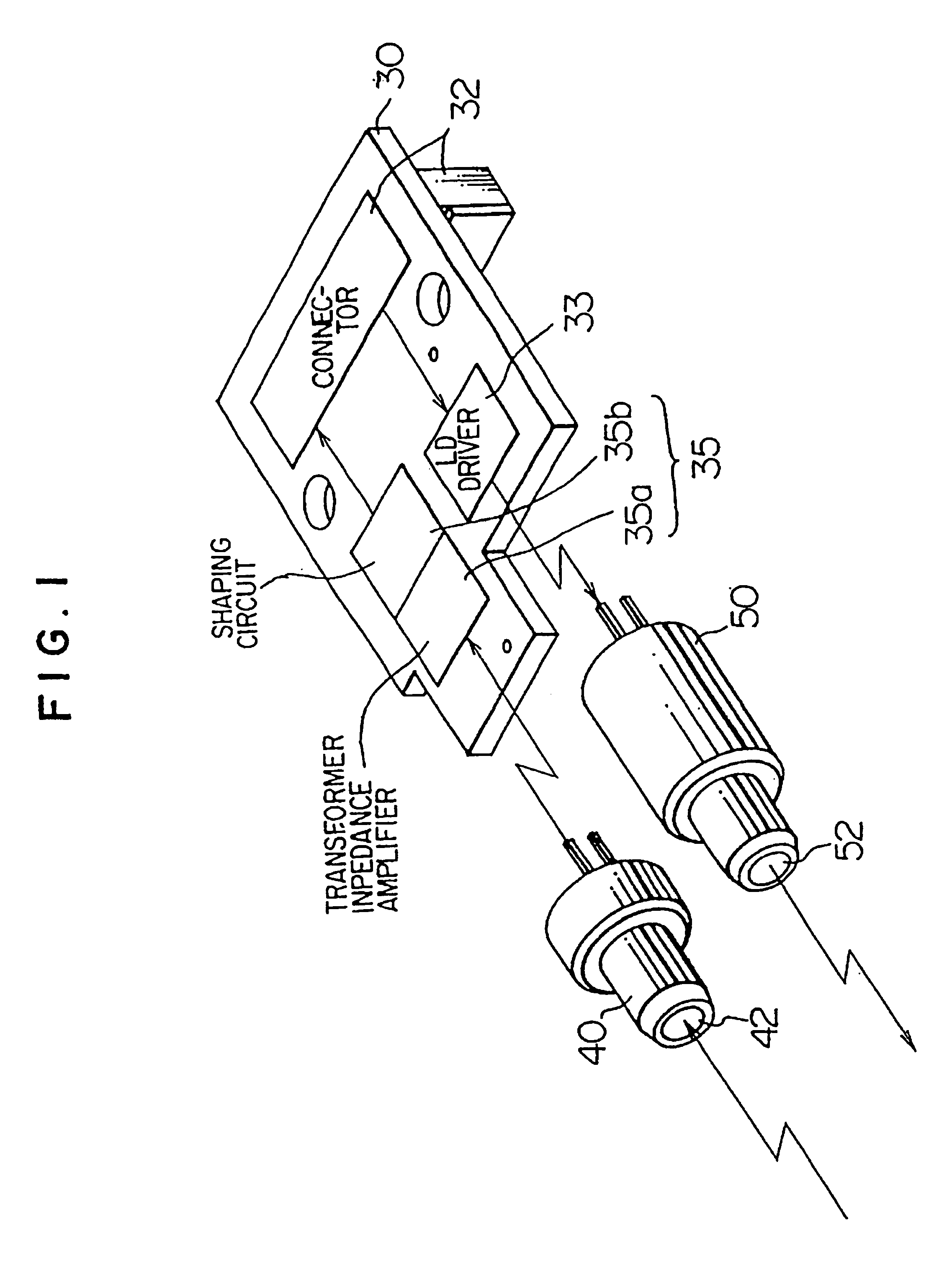
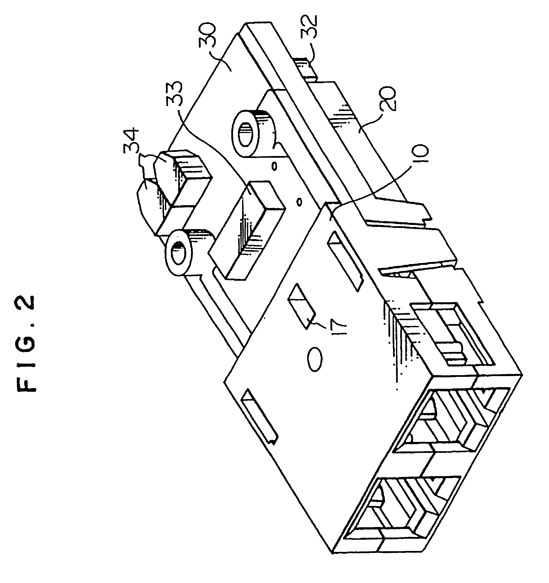
[0042]Referring first to FIG. 1, there is shown a block diagram of a fiber optic module in accordance with a first aspect of the present invention. In FIG. 1, a printed circuit board (which will be referred to as the PCB, hereinafter) 30 functions to send an electric signal (serial data) received at a PCB connector 32 to a laser diode (LD) driver 33 to drive an LD element (not shown and refer to FIG. 8) located within an LD module 50 and to transmit the data in the form of an optical signal to an optical fiber (ferule: not shown) inserted in an opening 52 of the LD module 50. A photodiode (PD) module 40, on the other hand, receives an optical signal from an optical fiber (not shown) inserted in an opening 42 of the PD module 40, converts the optical signal to a current through a PD element (not shown: refer to FIG. 8),...


PUM


Abstract

A fiber optic module includes a connector connected to a mother board of a host computer, an LD semiconductor IC for converting serial data received from the mother board to an LD electric signal for a laser diode, an LD module for converting the LD electric signal to an LD optical signal, a PD module for converting a photodiode optical signal to a PD electric signal, a PD semiconductor IC for converting the PD electric signal to PD serial data, a circuit board having the connector and carrying LD semiconductor IC and PD semiconductor IC, an LD shielding plate and a PD shielding plate for electrically shielding the LD module and the PD module, respectively, a first frame and a second frame for holding the circuit board, LD module and PD module. In the fiber optic module, the connector is of a surface mounting type, leads of the LD and PD modules are connected to a side of the circuit board mounted with the connector, the circuit board has an LD variable resistor for adjusting a drive current of the LD module, the LD variable resistor is provided to a side of the circuit board opposite to the connector, the circuit board has a PD variable resistor provided to the side of the circuit board opposite to the connector for detecting a signal of the PD module, 3 signal processing semiconductor ICs or less are provided.

Description

[0001]This is a continuation of application Ser. No. 09 / 087,857, which was filed on Jun. 1, 1998 to seek reissue of U.S. Pat. No. 5,596,663, which issued on Jan. 21, 1997 on application Ser. No. 08 / 372,078, filed on Jan. 12, 1995.[0002]More than one reissue application has been filed for the reissue of U.S. Pat. No. 5,596,663. The reissue applications are application Ser. No. 09 / 087,857, now U.S. Pat. No. Re 36,886, application Ser. No. 09 / 571,334, the present application, and application Ser. No. 10 / 766,488.BACKGROUND OF THE INVENTION[0003]The present invention relates to a fiber optic module which can be used in such a device as to perform data transfer between apparatuses.[0004]There has been so far known such a fiber optic module as shown in FIGS. 17-19 (disclosed in JP-A-3218134). FIG. 17 is a plan view of a prior art fiber optic module which comprises laser diode (LD) modules 1 for transmitting an optical signal onto a printed circuit board 3 having a width of 76 mm and a leng...

Claims


Application Information

Patent Timeline
Patent Type & Authority Patents(United States)
IPC IPC(8): G02B6/255G02B6/00G02B6/36G02B6/42H04B10/00
CPCG02B6/4246G02B6/4292H04B10/801
Inventor ISHIBASHI, SHINNAGAO, HIDEYUKIMIYAZAKI, TOMIYA
Owner II VI DELAWARE INC
Why Eureka
Try Eureka