

Epitaxial wafer and semiconductor element
a technology of semiconductor elements and epitaxial wafers, applied in the direction of crystal growth process, polycrystalline material growth, chemically reactive gases, etc., can solve the problems of increasing element resistance, reducing mobility, and reducing crystal quality of epitaxially-grown layers, so as to prevent the epitaxial quality from degrading, reduce the mobility of carriers, and reduce the effect of small element resistan
- Summary
- Abstract
- Description
- Claims
- Application Information
AI Technical Summary
Benefits of technology
Problems solved by technology
Method used
Image

Examples
first embodiment
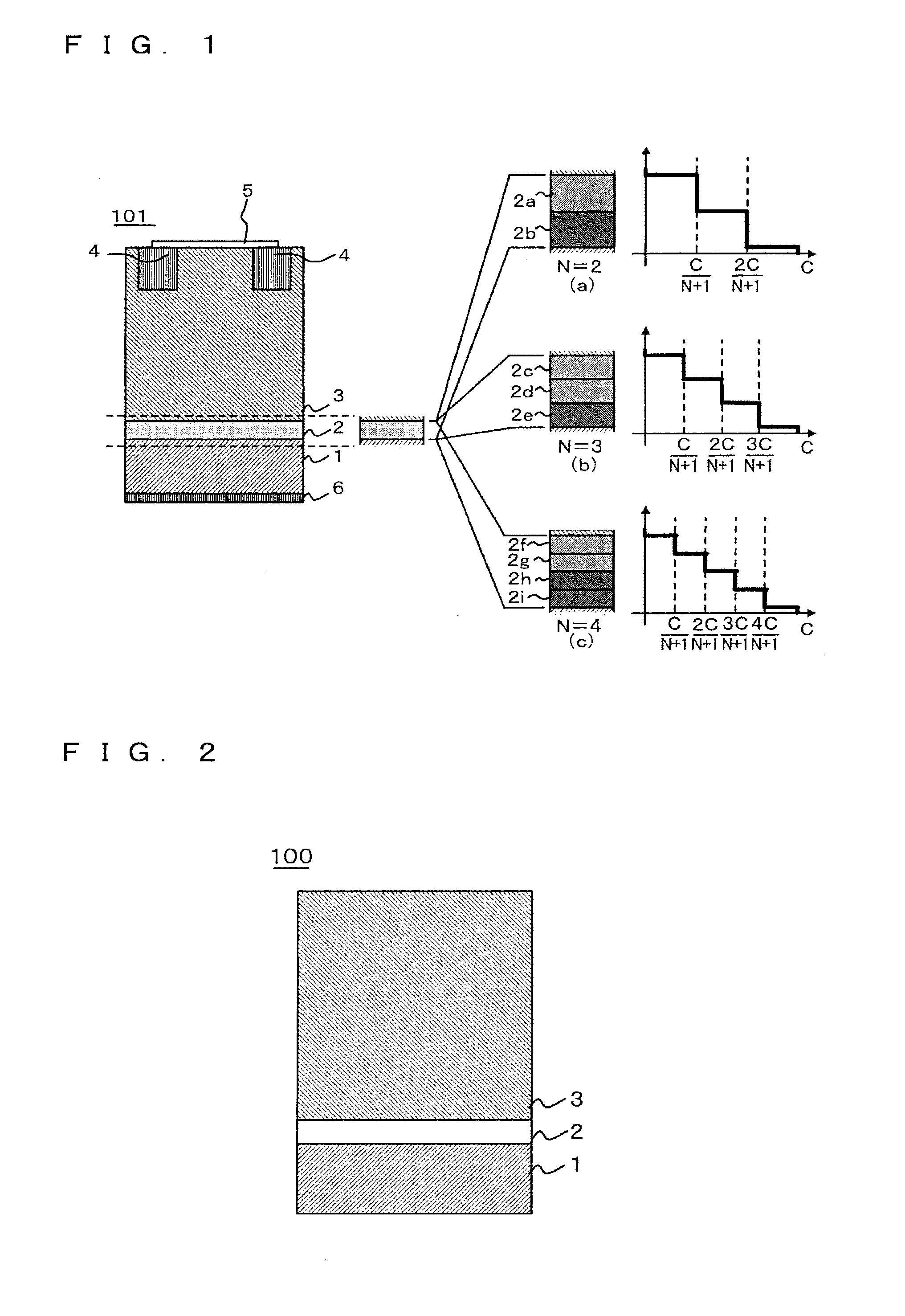
[0016]FIG. 1 is a cross-sectional view showing the configuration of a semiconductor element according to a first embodiment of the present invention. FIG. 2 is a cross-sectional view showing the configuration of an epitaxial wafer according to the first embodiment of the present invention.
[0017]With reference to FIG. 2, an epitaxial wafer 100 includes an n-type low-resistance silicon carbide substrate 1 of a first conductivity type that has an off-angle from a (0001) plane, an n-type buffer layer 2 formed on the silicon carbide substrate 1, and an epitaxially-grown layer 3 formed on the buffer layer 2 by epitaxial growth. The configuration of the buffer layer 2 is described below in detail.
[0018]With the use of the epitaxial wafer 100, a silicon carbide Schottky barrier diode 101 being the semiconductor element shown in FIG. 1 is formed. In the Schottky barrier diode 101, the epitaxially-grown layer 3 of the epitaxial wafer 100 serves as an n-type drift layer for maintaining the bre...
second embodiment
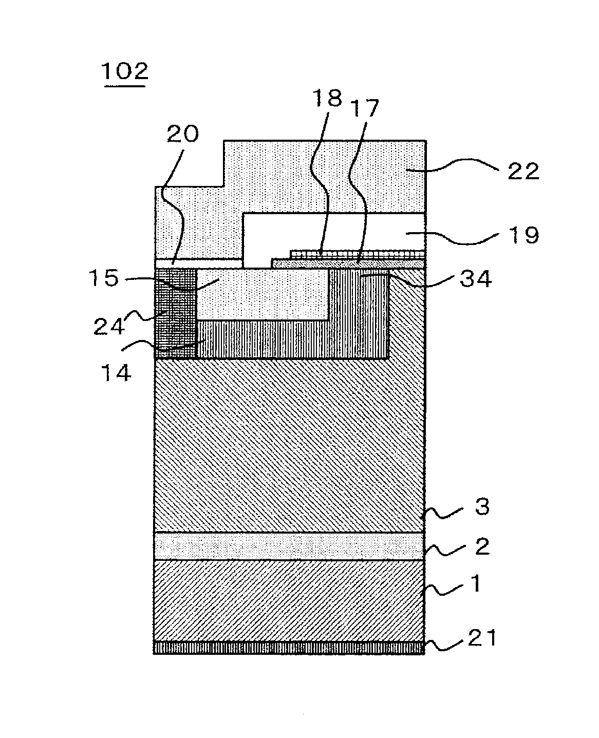
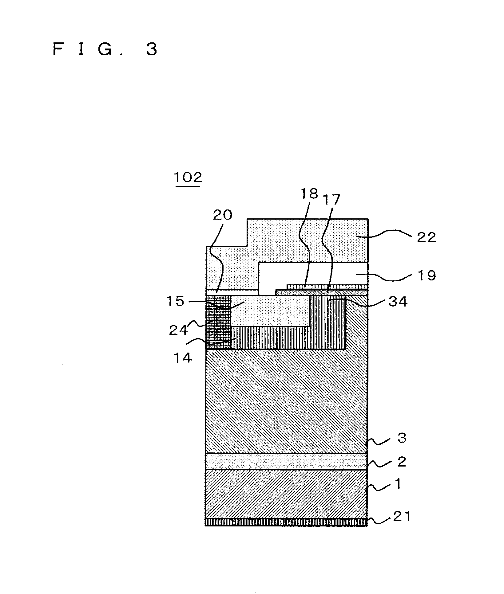
[0028]FIG. 3 is a cross-sectional view showing the configuration of a semiconductor element according to a second embodiment of the present invention.
[0029]With reference to FIG. 3, a silicon carbide MOSFET 102 being a semiconductor element is formed of the epitaxial wafer 100 including the n-type low-resistance silicon carbide substrate 1 having an off-angle from a (0001) plane, the n-type buffer layer 2 formed on the silicon carbide substrate 1, and the epitaxially-grown layer 3 formed on the buffer layer 2 by epitaxial growth, as in the first embodiment. Note that the configuration of the buffer layer 2 is similar to that of the first embodiment, and also similarly to the first embodiment, the epitaxially-grown layer 3 functions as an n-type silicon carbide drift layer for maintaining a breakdown voltage.
[0030]A p-type silicon carbide body region 14 and an n-type silicon carbide source region 15 are selectively formed in the n-type drift layer 3 by ion implantation and activation...
PUM
| Property | Measurement | Unit |
|---|---|---|
| thickness | aaaaa | aaaaa |
| thickness | aaaaa | aaaaa |
| thickness | aaaaa | aaaaa |
Abstract
Description
Claims
Application Information