Strained-silicon CMOS device and method

a strain-silicon, cmos technology, applied in the direction of semiconductor devices, basic electric elements, electrical equipment, etc., can solve the problems of metal oxide semiconductor transistors beginning to reach their traditional scaling limits, mobility degradation, carrier transport properties change, etc., to enhance the performance of devices fabricated, the effect of increasing the drive curren

Active Publication Date: 2005-12-29
GLOBALFOUNDRIES US INC
View PDF80 Cites 114 Cited by
  • Summary
  • Abstract
  • Description
  • Claims
  • Application Information

AI Technical Summary

Benefits of technology

[0023] Strain inducing wells comprising SiGe positioned within a biaxial compressively strained semiconducting layer and adjacent a device channel produce a compressive uniaxial strain within the device channel, wherein the uniaxial strain is in direction parallel to said device channel. The compressive uniaxial strain can provide carrier mobility enhancements in pFET devices.
[0042] The present invention also provides improved carrier mobility in semiconducting devices formed on a relaxed substrate, wherein a uniaxial strain parallel to the device channel of a transistor is provided by the combination of a strain inducing liner positioned atop the transistor and a strain inducing well positioned adjacent to the device channel. Broadly the inventive semiconductor structure comprises:

Problems solved by technology

However, there are growing signs today that metal oxide semiconductor transistors are beginning to reach their traditional scaling limits.
Since it has become increasingly difficult to improve MOSFETs and therefore CMOS performance through continued scaling, methods for improving performance without scaling have become critical.
This results in changes in carrier transport properties, which can be dramatic in certain cases.
It is believed that the reduction in drive currents in very short channel devices results from source / drain series resistance and that mobility degradation is due to higher channel doping by strong halo doping, velocity saturation, and self-heating.
In addition, in the case of biaxial tensile strain, such as strained epitaxially grown Si on relaxed SiGe, significant hole mobility enhancement for pFET devices only occurs when the device channel is under a high (>1%) strain, which is disadvantageously prone to have crystalline defects.

Method used


Image

  • Strained-silicon CMOS device and method
  • Strained-silicon CMOS device and method
  • Strained-silicon CMOS device and method

Examples


example 1

Formation of Compressive or Tensile Dielectric Capping Layer atop Biaxially Strained SGOI Substrate

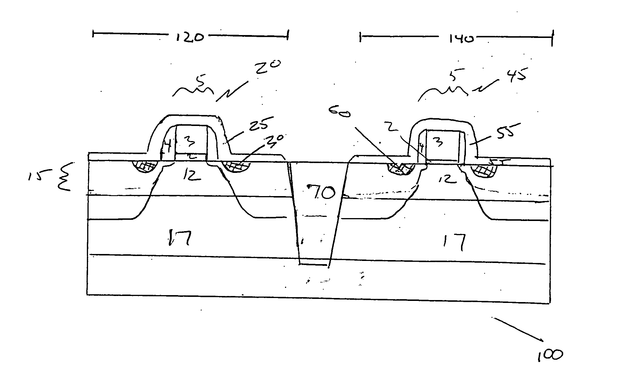
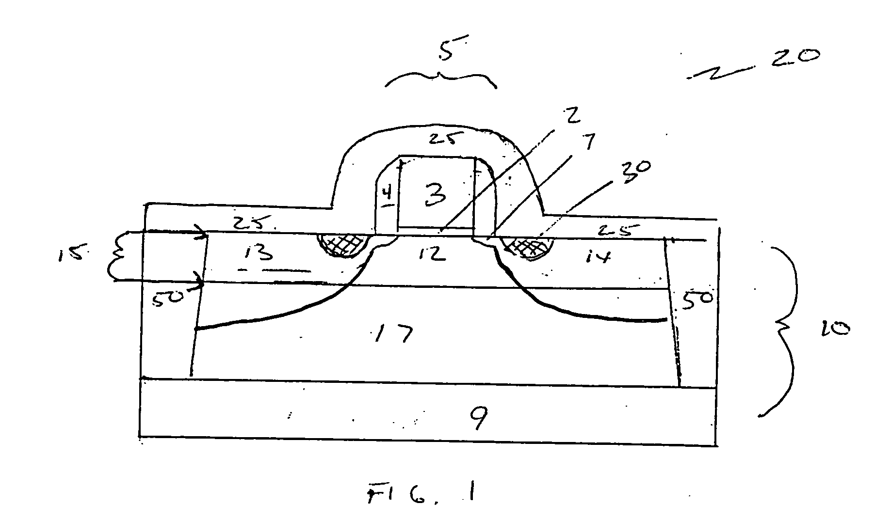
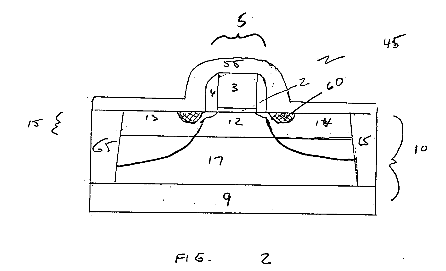
[0137] In this example, a dielectric capping layer (compressive or tensile strain inducing layer) was used to enhance the drive current by introducing a uniaxial strain along the FET channel. When such a dielectric capping layer is deposited over an SGOI FET, the lattice structure was distorted in response to the combination of a biaxial tensile strain and a smaller uniaxial tensile or compressive stress. FIG. 9(a) depicts a schematic description of biaxial tension strained Si, in which the longitudinal lattice dimension (x-direction, parallel to the channel) was equal to the transverse lattice dimension (y-direction, in the same plane and perpendicular to the device channel) and the normal lattice dimension (z-direction, out of the channel plane). FIG. 9(b) depicts the lattice symmetry of the biaxial tension strained Si substrate depicted in FIG. 9(a) with a superimposed uniaxial ten...


PUM


Abstract

The present invention provides a semiconductor device and a method of forming thereof, in which a uniaxial strain is produced in the device channel of the semiconductor device. The uniaxial strain may be in tension or in compression and is in a direction parallel to the device channel. The uniaxial strain can be produced in a biaxially strained substrate surface by strain inducing liners, strain inducing wells or a combination thereof. The uniaxial strain may be produced in a relaxed substrate by the combination of strain inducing wells and a strain inducing liner. The present invention also provides a means for increasing biaxial strain with strain inducing isolation regions. The present invention further provides CMOS devices in which the device regions of the CMOS substrate may be independently processed to provide uniaxially strained semiconducting surfaces in compression or tension.

Description

CROSS REFERENCE TO RELATED APPLICATION [0001] The present invention claims benefit of U.S. provisional patent application 60 / 582,678 filed Jun. 24, 2004, the entire content and disclosure of which is incorporated by reference.FIELD OF THE INVENTION [0002] The present invention relates to semiconductor devices having enhanced electron and hole mobilities, and more particularly, to semiconductor devices that include a silicon (Si)-containing layer having enhanced electron and hole mobilities. The present invention also provides methods for forming such semiconductor devices. BACKGROUND OF THE INVENTION [0003] For more than three decades, the continued miniaturization of silicon metal oxide semiconductor field effect transistors (MOSFETs) has driven the worldwide semiconductor industry. Various showstoppers to continued scaling have been predicated for decades, but a history of innovation has sustained Moore's Law in spite of many challenges. However, there are growing signs today that...

Claims


Application Information

Patent Timeline
Patent Type & Authority Applications(United States)
IPC IPC(8): H01L29/10H01L29/165H01L29/24
CPCH01L29/1054H01L29/165H01L29/7843H01L29/7842H01L29/24
Inventor BRYANT, ANDRESOUYANG, QIQINGRIM, KERN
Owner GLOBALFOUNDRIES US INC
Why Eureka
Try Eureka