Fully integrated organic layered processes for making plastic electronics based on conductive polymers and semiconductor nanowires

Inactive Publication Date: 2006-09-28
NANOSYS INC
View PDF41 Cites 113 Cited by
  • Summary
  • Abstract
  • Description
  • Claims
  • Application Information

AI Technical Summary

Benefits of technology

[0008] The present invention is directed to thin film transistors using nanowires, nanoribbons or other suitable nanostructures (e.g., nanorods, nanotubes and the like), and production scalable methods to produce such transistors using conductive polymer materials (e.g., polyaniline (PANI) or polypyrrole (PPY)) useful in the production of macroelectronics. In particular, an entirely new concept of macroelectronics has been developed by using oriented semiconductor nanowires, nanoribbons etc. incorporated in, on or within conductive polymer films to produce thin film transistors (TFTs) having high carrier mobility, with the conducting channel parallel to the wire/ribbon axis. Conducting polymers are particularly appealing for macroelectronic application

Problems solved by technology

While the current technology is successful in many perspectives, it is limited in what applications it can address.
However, the fabrication of high performance TFTs on plastics has been extremely challenging because all process steps must be carried out below the glass transition temperature of the plastic.
Significant efforts have been devoted to search for new materials (such as organics and organic-inorganic hybrids) or new fabrication strategies suitable for TFTs on plastics, but only with limited success.
Organic TFT's promise the potential of roll-to-roll fabrication pr

Method used


Image

  • Fully integrated organic layered processes for making plastic electronics based on conductive polymers and semiconductor nanowires
  • Fully integrated organic layered processes for making plastic electronics based on conductive polymers and semiconductor nanowires
  • Fully integrated organic layered processes for making plastic electronics based on conductive polymers and semiconductor nanowires

Examples


Example

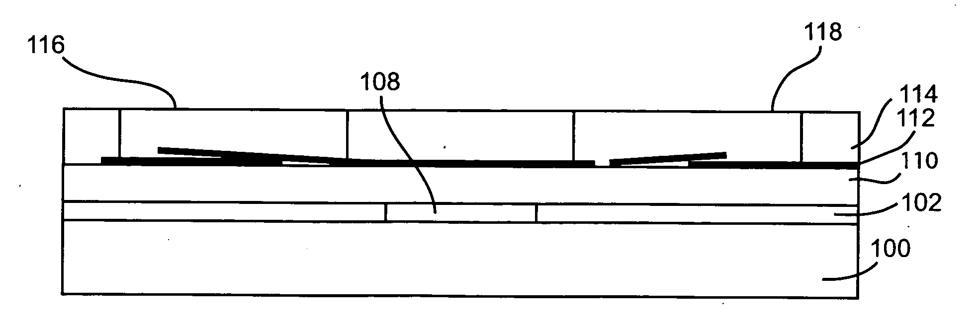
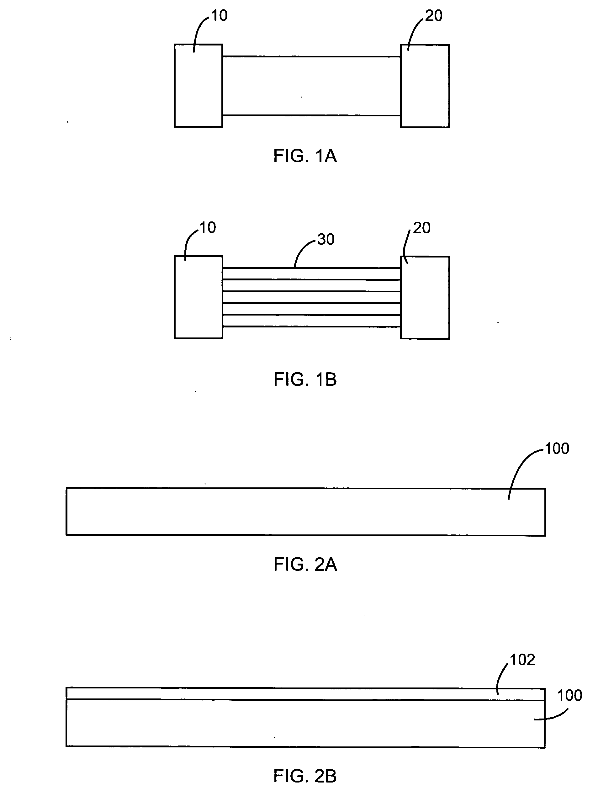
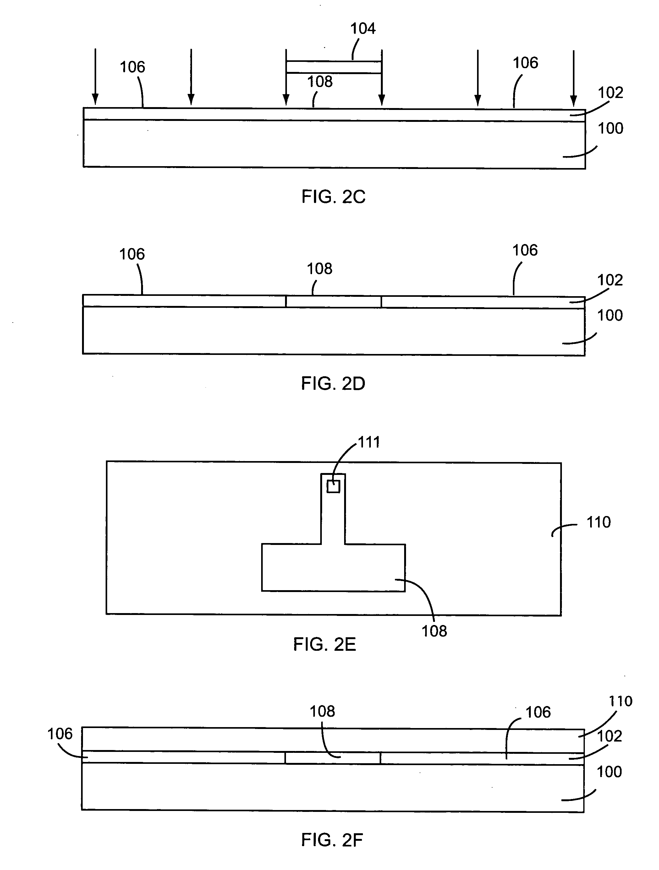
[0040] It should be appreciated that the particular implementations shown and described herein are examples of the invention and are not intended to otherwise limit the scope of the present invention in any way. Indeed, for the sake of brevity, conventional electronics, manufacturing, semiconductor devices, and nanotube, nanorod, nanowire and nanoribbon technologies and other functional aspects of the systems (and components of the individual operating components of the systems) may not be described in detail herein. Furthermore, for purposes of brevity, the invention is frequently described herein as pertaining to a semiconductor transistor device including nanowires. However, the present invention is not limited to nanowires, and other nanostructures such as nanotubes, nanorods, nanowhiskers, nanoribbons and the like may be used. Moreover, while the number of nanowires and spacing of those nanowires are provided for the specific implementations discussed, the implementations are n...


PUM

PropertyMeasurementUnit
Electrical conductoraaaaaaaaaa
Plasticityaaaaaaaaaa

Abstract

The present invention is directed to thin film transistors using nanowires (or other nanostructures such as nanoribbons, nanotubes and the like) incorporated in and/or disposed proximal to conductive polymer layer(s), and production scalable methods to produce such transistors. In particular, a composite material comprising a conductive polymeric material such as polyaniline (PANI) or polypyrrole (PPY) and one or more nanowires incorporated therein is disclosed. Several nanowire-TFT fabrication methods are also provided which in one exemplary embodiment includes providing a device substrate; depositing a first conductive polymer material layer on the device substrate; defining one or more gate contact regions in the conductive polymer layer; depositing a plurality of nanowires over the conductive polymer layer at a sufficient density of nanowires to achieve an operational current level; depositing a second conductive polymer material layer on the plurality of nanowires; and forming source and drain contact regions in the second conductive polymer material layer to thereby provide electrical connectivity to the plurality of nanowires, whereby the nanowires form a channel having a length between respective ones of the source and drain regions.

Description

CROSS-REFERENCE TO RELATED APPLICATIONS [0001] This application claims priority to U.S. Provisional Patent Application No. 60 / 617,830, filed Oct. 12, 2004, the entirety of which is incorporated herein.STATEMENT REGARDING FEDERALLY SPONSORED RESEARCH [0002] Not applicable. BACKGROUND OF THE INVENTION [0003] The present invention relates to semiconductor devices, and more particularly, to the fabrication and use of novel electronic devices made using conductive polymer materials having nanowires (or other nanostructures) incorporated therein and / or thereon. [0004] The advancement of electronics has been moving towards two extremes in terms of physical scale. Rapid miniaturization of microelectronics according to Moore's law has led to remarkable increases in computing power while at the same time enabling reductions in cost. In parallel, extraordinary progress has been made in the other, relatively less noticed, area of macroelectronics, where electronic devices are integrated over la...

Claims


Application Information

Patent Timeline
IPC IPC(8): H01L29/08
CPCB82Y10/00H01L29/0673H01L29/068H01L29/78681H01L29/7869H01L29/78696H01L51/0035H01L51/0037H01L51/0048H01L51/0049H01L51/0541H01L51/0545H01L51/0566H01L51/4253H01L51/4266Y02E10/549Y10S977/762Y10S977/763Y10S977/764Y02P70/50H10K85/111H10K85/225H10K85/1135H10K85/221H10K10/488H10K10/464H10K10/466H10K30/352H10K30/30
Inventor PAN, YAOLINGLEON, FRANCISCOSTUMBO, DAVID P.
Owner NANOSYS INC
Why Eureka
Try Eureka