III-nitride semiconductor device with trench structure

Active Publication Date: 2005-07-07
INFINEON TECH AMERICAS
View PDF8 Cites 118 Cited by
  • Summary
  • Abstract
  • Description
  • Claims
  • Application Information

AI Technical Summary

Benefits of technology

[0018] In accordance with the present invention, there is provided a nominally off, or enhancement mode FET device, realized in a III-nitride material system. The FET is capable of carrying high currents

Problems solved by technology

The nominally on nature of the HEMT devices previously fabricated have limited their applicability to power management.
The limitations of nominally on power devices is observed in the need to have a control circuit powered and operational, before power can be safely controlled by a nominally on device.
A drawback of III-nitride devices that permit high current densities with low resistive losses is the limited thickness that can be achieved in the strained AlGaN/GaN system.
The difference in the lattice structures of these types of materials produces a strain that can result in dislocation of films grown to produce the different layers.
This results in high levels of leakage through a barrier layer, for example.
However, the problem of limited thickness is not addressed by these designs.
While additional insulator layers can permit thicker strained AlGaN/GaN systems to be constructed, the confinement layer produced by the additional insulator results in lower current carrying capacity due to the scattering effect produced on electrons at the GaN/insulator interface.
Also, the additional interface between the Al

Method used


Image

  • III-nitride semiconductor device with trench structure
  • III-nitride semiconductor device with trench structure
  • III-nitride semiconductor device with trench structure

Examples


Embodiment Construction

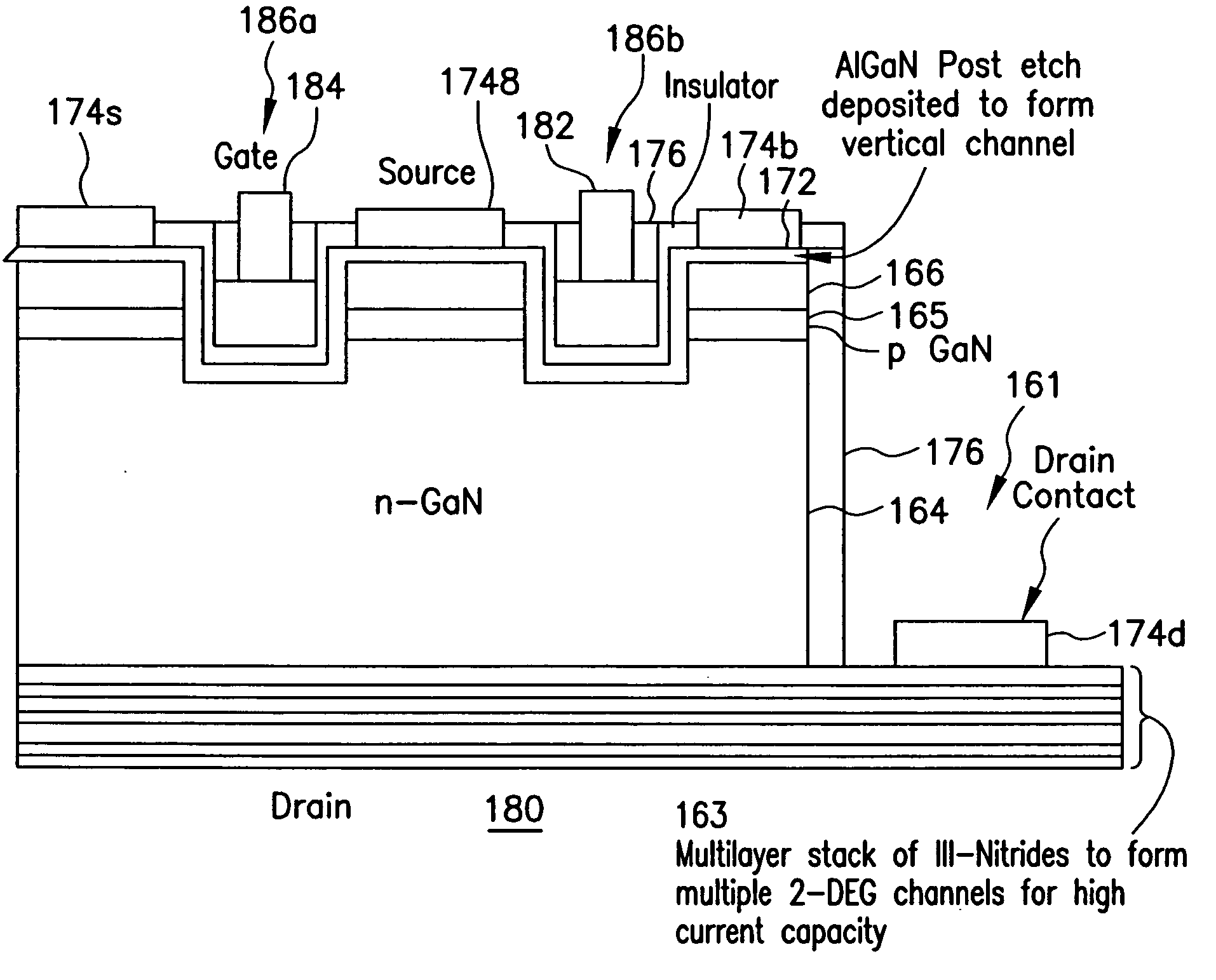
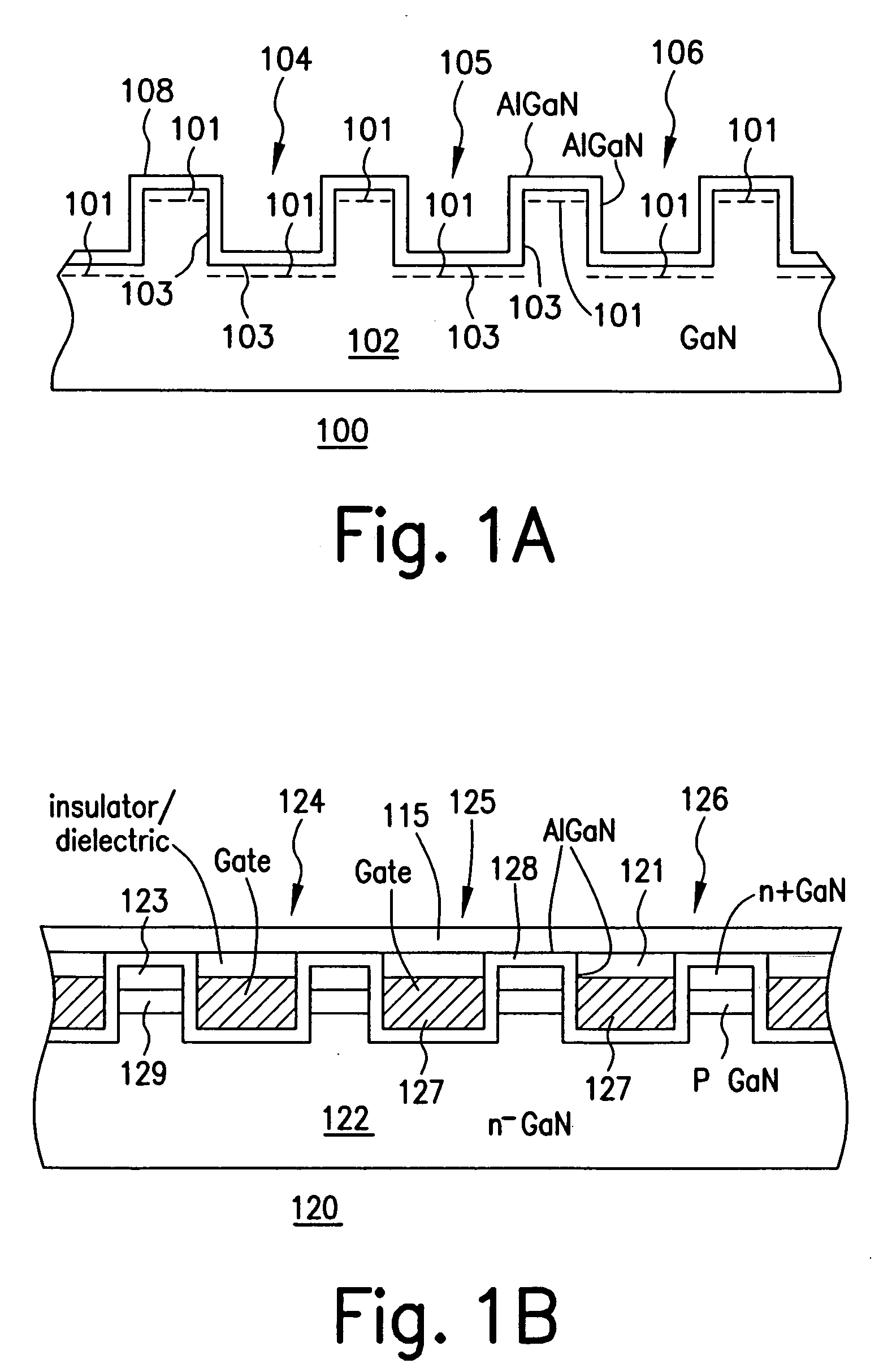
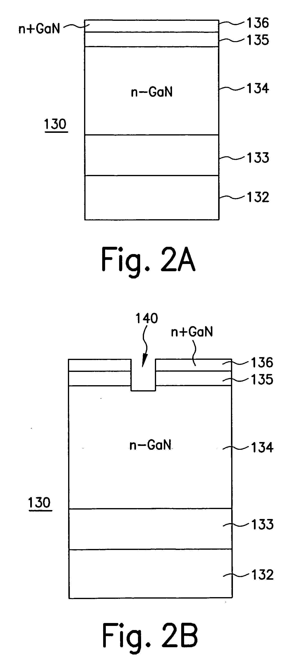
[0053] In the construction of GaN material devices, a number of factors come into play to impact the functionality and capability of the devices. A large lattice mismatch in III-nitride materials and the strong piezoelectric and polarization effects in these materials significantly impact the electrical properties of III-nitride heterojunction devices. A significant number of reported GaN-based devices to date use strained GaN / AlGaN junctions with alloy compositions that are designed to relieve the strain to avoid dislocations that may be responsible for long term instabilities in the devices. Various devices and systems for building heterojunction devices have been proposed to control the lattice mismatch and the strain of the GaN / AlGaN junctions. These devices are particularly designed to take advantage of piezoelectric and spontaneous polarization effects and to minimize long term instabilities.

[0054] GaN / AlGaN devices typically have one or more terminals for controlling electri...


PUM


Abstract

A III-nitride trench device has a vertical conduction region with an interrupted conduction channel when the device is not on, providing an enhancement mode device. The trench structure may be used in a vertical conduction or horizontal conduction device. A gate dielectric provides improved performance for the device by being capable of withstanding higher electric field or manipulating the charge in the conduction channel. A passivation of the III-nitride material decouples the dielectric from the device to permit lower dielectric constant materials to be used in high power applications.

Description

RELATED APPLICATION [0001] The present application is based on and claims benefit of U.S. Provisional Application No. 60 / 527,636, filed Dec. 5, 2003, entitled III-Nitride MISFIT, and U.S. Provisional Application No. 60 / 549,639, filed Mar. 3, 2004, entitled Vertical Channel III-Nitride and U.S. Provisional Application No. 60 / 623,678, filed Oct. 29, 2004, entitled III-Nitride Semiconductor Device With Trench Structure, to all of which a claim of priority is hereby made, and the disclosures of which are hereby incorporated herein by reference.BACKGROUND OF THE INVENTION [0002] 1. Field of the Invention [0003] The present invention relates generally to a trench device realized in a III-nitride material system, and relates more particularly to a class of trench switching devices that are nominally off in a III-nitride material system. [0004] 2. Description of Related Art [0005] III-nitride semiconductors are presently known that exhibit a large dielectric breakdown field of greater than ...

Claims


Application Information

Patent Timeline
IPC IPC(8): H01L21/336H01L21/338H01L29/812H01L29/12H01L29/778H01L29/78H01L29/80H01L29/808H01L31/0328
CPCH01L29/0696H01L29/7835H01L29/2003H01L29/4236H01L29/51H01L29/517H01L29/518H01L29/66462H01L29/66522H01L29/66734H01L29/7787H01L29/7788H01L29/7789H01L29/7813H01L29/0847
Inventor BEACH, ROBERTBRIDGER, PAUL
Owner INFINEON TECH AMERICAS
Why Eureka
Try Eureka