Methods to fabricate thin film transistors and circuits

Inactive Publication Date: 2001-05-01
MCGILL UNIV OFFICE OF TECH TRANSFER
View PDF2 Cites 117 Cited by
  • Summary
  • Abstract
  • Description
  • Claims
  • Application Information

AI Technical Summary

Problems solved by technology

Hence the power consumption for the deposition of Si films is high.
Furthermore, the deposition of uniform Si films on substrates with relatively large dimensions required for the electronic displays is difficult to achieve due to the distribution of molecules in the reaction chamber.
Although some success has been demonstrated in the prior art, it has been observed that the rep

Method used


Image

  • Methods to fabricate thin film transistors and circuits
  • Methods to fabricate thin film transistors and circuits
  • Methods to fabricate thin film transistors and circuits

Examples


Embodiment Construction

Fabrication Processes for TFTs with CBD Deposited CdS films

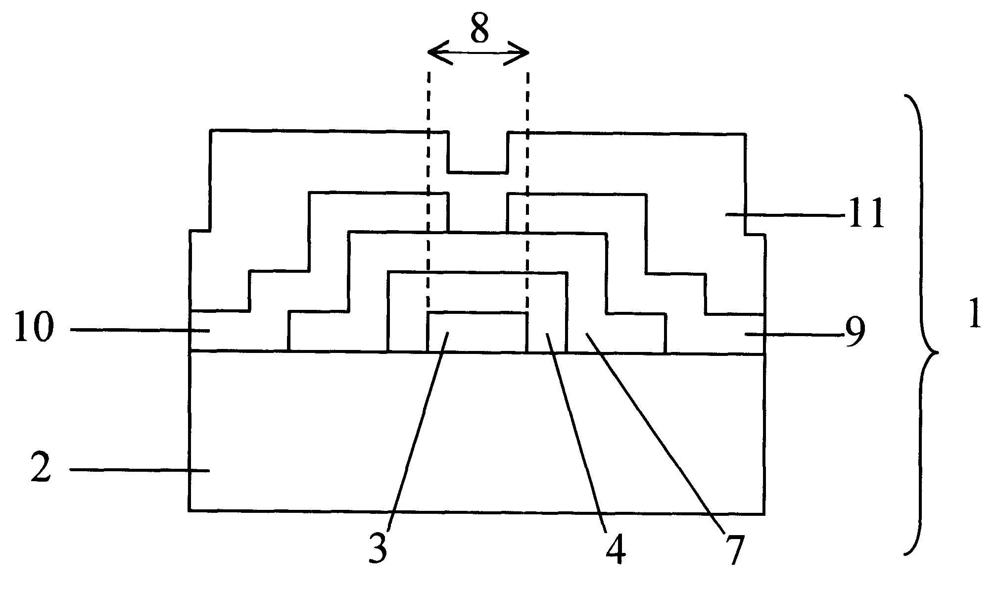
Referring to FIG. 1(a), where there is shown a TFT (1) embodiment. A glass plate (2) with a thickness of 1 mm is used as the substrate. A layer of metal (3) such as Al or Ta is deposited by standard vacuum deposition method and then patterned to form gate. A layer of dielectric layer (4) is deposited. This dielectric layer may be in a form of Ta.sub.2 O.sub.5, TaO.sub.x or Al.sub.2 O.sub.3 which is deposited by an anodization method. Alternately, it may be SiO.sub.2, SiN.sub.x, Si.sub.3 N.sub.4, TiO.sub.2, Ta.sub.2 O.sub.5, TaO.sup.x or Al.sub.2 O.sub.3 and deposited by a CVD method. The thickness of the dielectric layer should be large enough, more than 30 nm, so that leakage current through this dielectric layer is minimized but is not too large, less than 500 nm, to give rise to an excessive threshold voltage of the thin film transistor. Due to the nature of the anodization process, only the surfaces of the metal layer (3...


PUM


Abstract

A method for fabricating a thin film field effect transistor is described in this invention. The active layer of the thin film transistor (TFT) is formed by a low cost chemical bath deposition method. The fabrication procedure includes deposition of a metal layer on an insulating substrate, patterning of the metal layer to form a metal gate, formation of the di-electric layer, deposition of the active layer and formation of source and drain contacts.

Description

[1] FIELD OF INVENTIONThis invention relates to a thin film transistor, a circuit of thin film transistors and a low cost method of making the same.[2] BACKGROUND OF THE INVENTIONIn flat panel electronic displays, light switching elements are arranged in a two dimensional array where the optical state of each element (or pixel) is controlled by at least one transistor. In addition to the transistors used to control the optical state of pixels, transistors are required to form column driving circuit and row driving circuit which control the flow of electrical signals to individual pixels. Since most of the flat panel electronic displays are fabricated on low cost glass substrates, the transistors used to control the optical state and the transistors to form the row and column driving circuits are usually in a thin film form. The active region of conventional thin film transistor is a layer of semiconductor. There are several requirements for a thin film transistor used in high qualit...

Claims


Application Information

Patent Timeline
IPC IPC(8): H01L21/336H01L21/02H01L29/66H01L29/786
CPCH01L29/66765H01L29/78609
Inventor GAN, FENG YUANSHIH, ISHIANG
Owner MCGILL UNIV OFFICE OF TECH TRANSFER
Why Eureka
Try Eureka