Semiconductor device having a channel layer and method of manufacturing the same

a technology of semiconductor devices and channel layers, which is applied in semiconductor devices, electrical devices, instruments, etc., can solve the problems of delta mos transistors, single-crystalline layers damaged, and increased junction capacitance between source and drain regions, so as to improve the mobility of carrier channels and improve the operating characteristics.

Inactive Publication Date: 2005-12-01
SAMSUNG ELECTRONICS CO LTD
View PDF18 Cites 128 Cited by
  • Summary
  • Abstract
  • Description
  • Claims
  • Application Information

AI Technical Summary

Benefits of technology

[0016] Accordingly, the present invention provides a semiconductor device for improving carrier mobility.
[0023] In an embodiment of the present invention, an advantage is that the carrier mobility of the channel layer can be remarkably improved as compared with a conventional channel layer; thus a driving current of the semiconductor device increases to thereby improve operating characteristics.

Problems solved by technology

However, the fin structured MOS transistor is disadvantageous in that a plurality of channel fins is arranged in parallel along a width direction of the gate; thus the channel region and the source / drain regions are enlarged in the MOS transistor.
Another drawback of the fin structured MOS transistor is that junction capacitance between the source and drain regions is increased as the channel number is increased.
However, the DELTA MOS transistor has disadvantages as follows.
In addition, a single-crystalline layer is damaged due to a stress during the over-oxidation process.
However, there is a problem that the channel width is limited by the thickness of the SOI layer.
However, the GAA MOS transistor also has problems as follows.

Method used


Image

  • Semiconductor device having a channel layer and method of manufacturing the same
  • Semiconductor device having a channel layer and method of manufacturing the same
  • Semiconductor device having a channel layer and method of manufacturing the same

Examples


Embodiment Construction

[0032] The present invention now will be described more fully hereinafter with reference to the accompanying drawings in which exemplary embodiments of the present invention are shown.

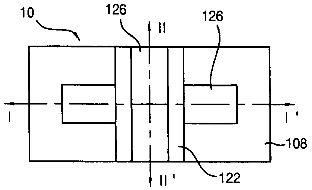
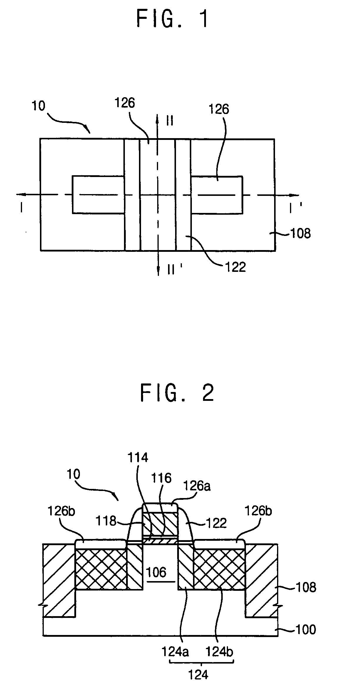
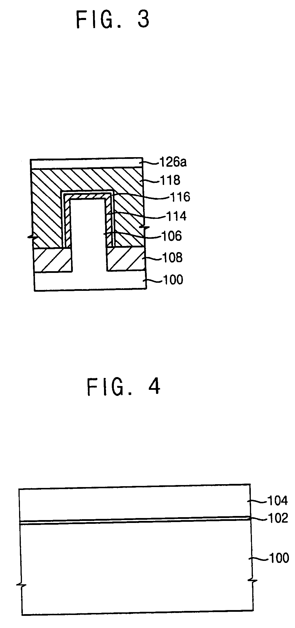
[0033]FIG. 1 is a plan view illustrating a semiconductor device according to an exemplary embodiment of the present invention. FIG. 2 is a cross sectional view taken along the line I-I′ of the semiconductor device shown in FIG. 1, and FIG. 3 is a cross sectional view taken along the line II-II′ of the semiconductor device shown in FIG. 1.

[0034] Referring to FIGS. 1 to 3, the semiconductor device 10 according to an exemplary embodiment of the invention includes a fin body 106 protruded from a substrate 100 such as a silicon wafer. The fin body 106 extends in a first direction (e.g., along or parallel to line I-I′) across the substrate 100, and is surrounded by a field insulation pattern 108. A conventional shallow trench isolation (STI) process may exemplarily be utilized for the field insulation patt...


PUM

PropertyMeasurementUnit
dielectric constantaaaaaaaaaa
conductiveaaaaaaaaaa
structureaaaaaaaaaa

Abstract

In a method of forming a semiconductor device having an improved channel layer, the channel layer is formed on a surface of a semiconductor substrate and comprises a material of high carrier mobility such as silicon germanium (SiGe), germanium (Ge) and silicon carbide (SiC) using a selective epitaxial growth process. A gate insulation layer and a gate electrode are formed on the channel layer. Accordingly, a driving current of the semiconductor device increases to thereby improve operation characteristics.

Description

CROSS-REFERENCE TO RELATED APPLICATION [0001] This application relies for priority upon Korean Patent Application No. 2004-37470 filed on May 25, 2004, the content of which is herein incorporated by reference in its entirety. BACKGROUND OF THE INVENTION [0002] 1. Field of the Invention [0003] The present invention relates to a semiconductor device having a channel layer and a method of manufacturing the same. More particularly, the present invention relates to a semiconductor device such as a field effect transistor (FET) and a method of manufacturing the same. [0004] 2. Description of the Related Art [0005] As semiconductor devices are highly integrated, an active region in which various conductive structures are positioned has been reduced in a size and a channel length of the MOS transistor in the active region has been also shortened. When the channel length is shortened, a voltage applied to a source or a drain of the MOS transistor has much more effect on an electrical field i...

Claims


Application Information

Patent Timeline
Patent Type & Authority Applications(United States)
IPC IPC(8): H01L21/335H01L21/336H01L29/78H01L29/76H01L29/786
CPCH01L29/66795H01L29/78687H01L29/785G07F19/20G07D2211/00
Inventor CHOI, JEONG-DONGOH, CHANG-WOOPARK, DONG-GUNKIM, DONG-WON
Owner SAMSUNG ELECTRONICS CO LTD
Why Eureka
Try Eureka