Fabrication of strained heterojunction structures

a heterojunction structure and semiconductor technology, applied in the field of semiconductor processing, can solve the problems of difficult to have adjacent devices in different strain states, rough growth front, and high-quality strained silicon, and achieve the effects of improving carrier mobility, improving characteristics, and improving speed

Active Publication Date: 2006-06-22
WISCONSIN ALUMNI RES FOUND
View PDF27 Cites 137 Cited by
  • Summary
  • Abstract
  • Description
  • Claims
  • Application Information

AI Technical Summary

Benefits of technology

[0006] In accordance with the present invention, growth of multilayer films is carried out in a manner which allows close control of the strain in the grown layers and complete release of the grown films to allow mounting of the released multilayer structure on selected substrates. The released multilayer structures can be formed as discrete individual sections that can be placed at desired locations on a permanent substrate, or the structure can be released as a large, flexible film that can be mounted over a large-area substrate, including substrates with non-planar surfaces. The invention enables fabrication of electronic devices with improved characteristics, taking advantage of heterojunctions in which one or both of the adjacent layers is strained to significantly increase carrier mobility. Examples of devices that may be formed utilizing the invention include high-mobility modulation-doped field-effect transistors, wherein a strained silicon layer is utilized as a carrier channel clad with a silicon-germanium alloy in which the final strain state is achieved by elastic strain sharing between the films, and imaging and computing devices having higher speeds due to increased carrier mobility.

Problems solved by technology

The main obstacle to obtaining high-quality strained silicon is initially in obtaining a perfect strain-relaxed SiGe film.
The difficulty with dislocation-driven relaxation is that every misfit dislocation has two threading arms associated with the dislocation.
A further limitation with the use of graded SiGe substrates is that to achieve few dislocations in the Si layer, it is necessary to grow very thick graded SiGe films.
However, the relatively thick films make it difficult to have adjacent devices that are in different strain states.
These steps have a tendency to bunch together, creating a rough growth front.
A polishing and cleaning step must be carried out before growing the silicon layer, adding cost to the processing.
Thermal conductivity is also poor through the graded layers.
The problem with the compliant-substrate approach is that it is very difficult to achieve a truly compliant substrate, since doing so requires a large-scale slipping between the strained system and the compliant layer.
The supported mesas formed in this manner are fixed in location and are limited in the surface area available for device formation.

Method used


Image

  • Fabrication of strained heterojunction structures
  • Fabrication of strained heterojunction structures
  • Fabrication of strained heterojunction structures

Examples


Embodiment Construction

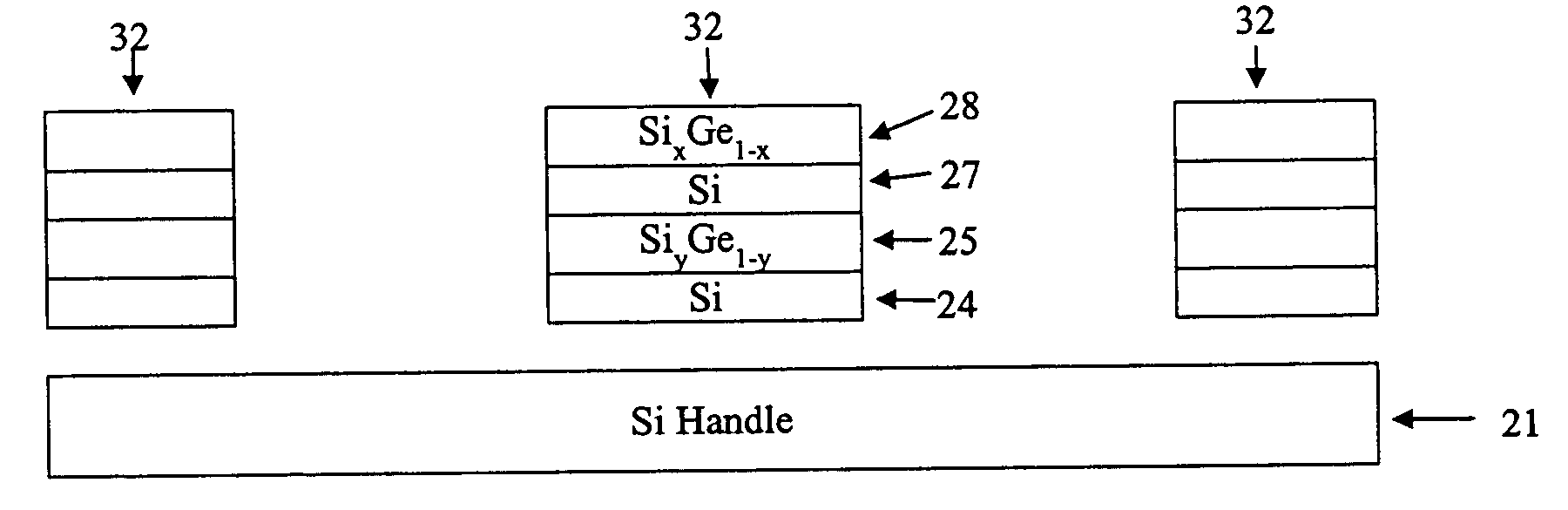
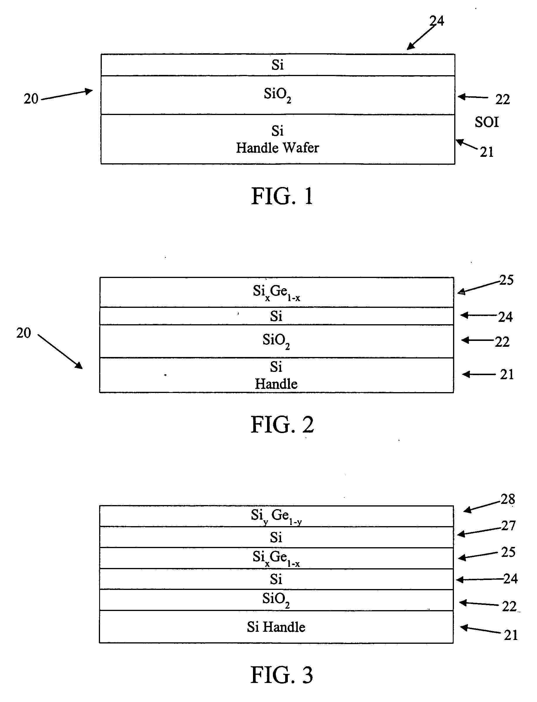
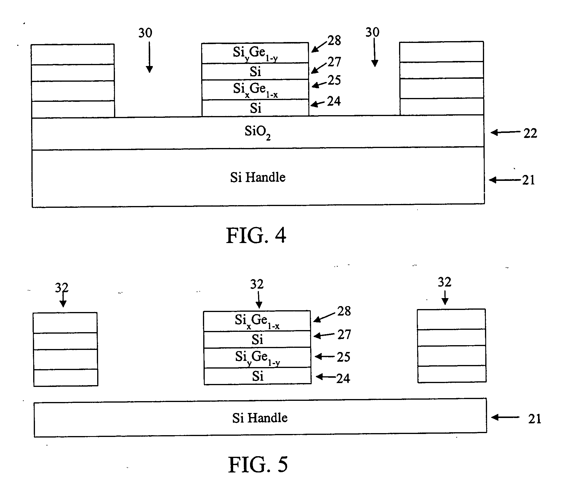
[0030] The present invention provides a new approach for controlling strain in heterostructures. For purposes of exemplifying the invention, the following describes the production of silicon / silicon-germanium heterostructures which are formed on silicon-on-insulator (SOI) substrates and then released, but the invention may be implemented in any semiconductor system or other material system requiring strain control as discussed herein.

[0031] An initial SOI wafer is shown generally in cross-section at 20 in FIG. 1 and includes a crystalline silicon handle wafer 21, an insulating (sacrificial) layer 22 of SiO2, and a template layer 24 of crystalline silicon that is typically 10 to 100 nm thick. As shown in FIG. 2, an initial layer 25 of SiGe is grown epitaxially on the silicon template layer 24 by any suitable process, such as molecular beam epitaxy (MBE), chemical vapor deposition (CVD), sputter deposition, etc., with the SiGe layer 25 in a state of internal compressive strain as gro...


PUM


Abstract

Growth of multilayer films is carried out in a manner which allows close control of the strain in the grown layers and complete release of the grown films to allow mounting of the released multilayer structures on selected substrates. A layer of material, such as silicon-germanium, is grown onto a template layer, such as silicon, of a substrate having a sacrificial layer on which the template layer is formed. The grown layer has a lattice mismatch with the template layer so that it is strained as deposited. A top layer of crystalline material, such as silicon, is grown on the alloy layer to form a multilayer structure with the grown layer and the template layer. The sacrificial layer is preferentially etched away to release the multilayer structure from the sacrificial layer, relaxing the grown layer and straining the crystalline layers interfaced with it.

Description

REFERENCE TO GOVERNMENT RIGHTS [0001] This invention was made with United States government support awarded by the following agency: NSF 0079983. The United States government has certain rights in this invention.FIELD OF THE INVENTION [0002] This invention pertains generally to the field of semiconductor processing and particularly to the formation of strained heterojunction semiconductor structures. BACKGROUND OF THE INVENTION [0003] Controlling the strain and the number and type of defects in heteroepitaxial semiconductor structures is crucial for obtaining high-quality semiconductor materials with the desired properties for forming high-performance devices. In the silicon / silicon-germanium hetero-system, appropriate control of the strain in the semiconductor layers provides control over band offsets and carrier mobility. Typically, it is desirable to be able to obtain a strain-relaxed SiGe virtual substrate on which a thin strained Si film is formed. The main obstacle to obtainin...

Claims


Application Information

Patent Timeline
Patent Type & Authority Applications(United States)
IPC IPC(8): H01L21/20H01L21/302
CPCH01L21/6835H01L21/76256H01L21/84H01L29/0657H01L2221/6835
Inventor SAVAGE, DONALD E.ROBERTS, MICHELLE M.LAGALLY, MAX G.
Owner WISCONSIN ALUMNI RES FOUND
Why Eureka
Try Eureka