Infrared sensor ic, and infrared sensor and manufacturing method thereof

Active Publication Date: 2007-04-26
ASAHI KASEI ELECTRONICS CO LTD
View PDF9 Cites 34 Cited by
  • Summary
  • Abstract
  • Description
  • Claims
  • Application Information

AI Technical Summary

Benefits of technology

[0029] Since a subminiature human sensor that can be operated at room temperature can be provided by employing the infrared sensor IC for one mode of the invention, this sensor can be easily mounted on a home electrical appliance for which the mounting of a sensor is conventionally difficult. According to the infrared sensor IC of the mode of this invention, by hybrid formation with the integrated circuit, a quantum infrared sensor, for which cooling is conventionally required and wherein a compound semiconductor that is practicall

Problems solved by technology

And in addition, since the infrared sensor and the integrated circuit are arranged using hybrid formation, they a

Method used


Image

  • Infrared sensor ic, and infrared sensor and manufacturing method thereof
  • Infrared sensor ic, and infrared sensor and manufacturing method thereof
  • Infrared sensor ic, and infrared sensor and manufacturing method thereof

Examples


first embodiment

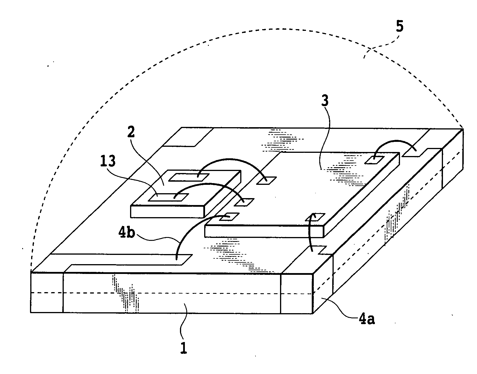
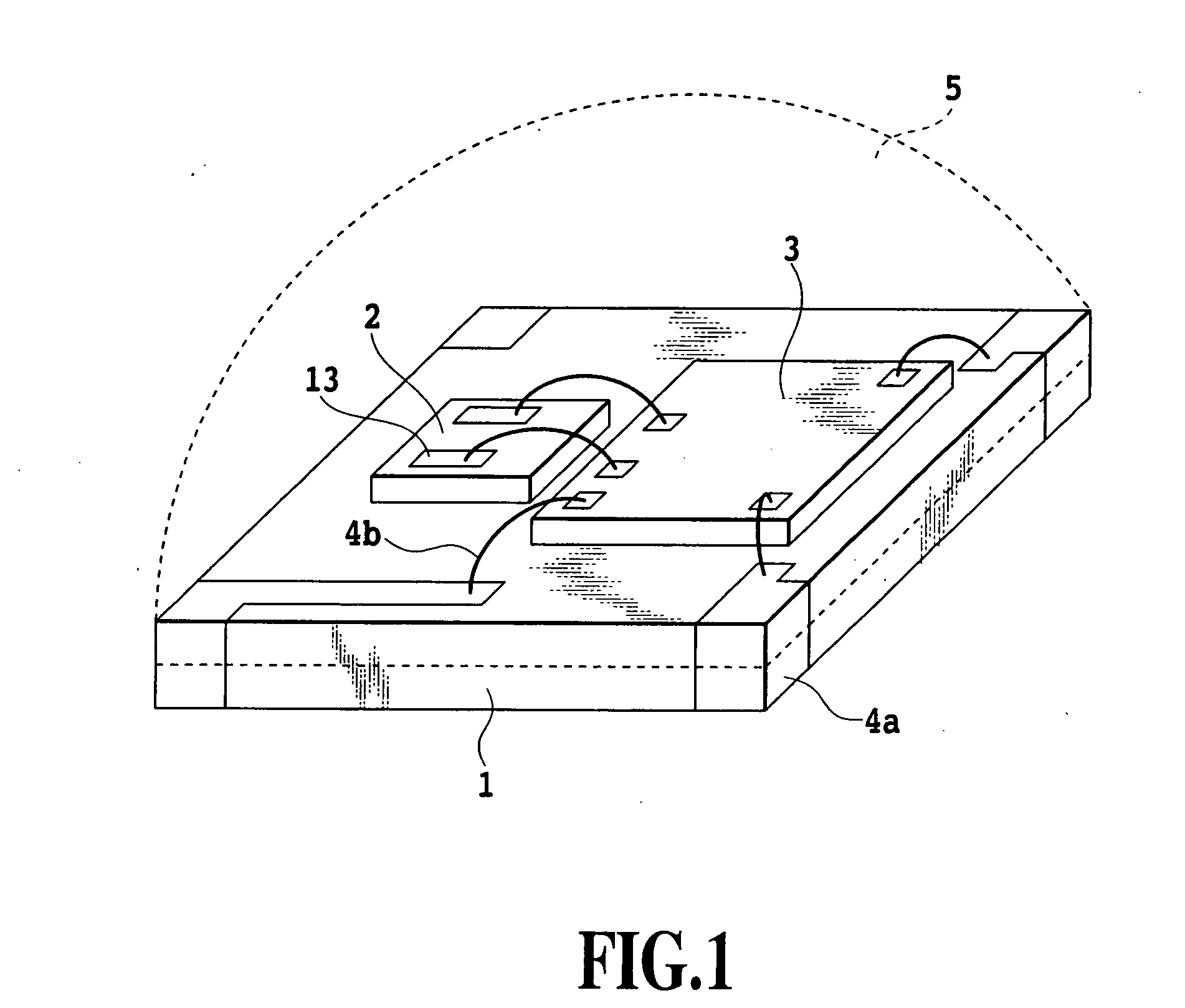
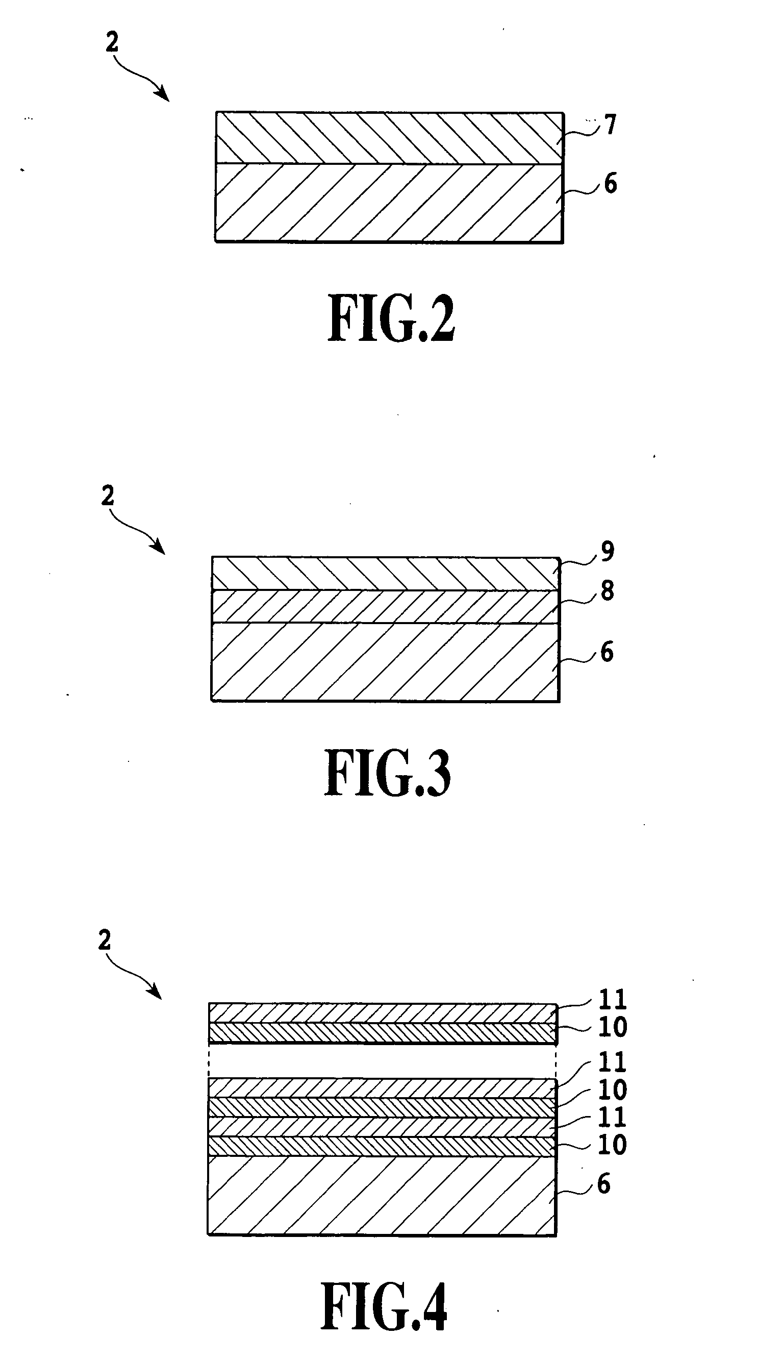
[0126] Using the MBE method, non-doped InAs0.23Sb0.77 of 2 μm was grown on a GaAs substrate. The film characteristics of a thin InAsSb film were measured using the van der Pauw method, and an electron mobility of 35,000 cm2 / Vs at room temperature, a sheet resistance (device resistance) of 20 Ω, and a carrier density of 1×10¹⁷ atoms / cm3 were obtained. A compound semiconductor sensor was then fabricated by using this thin compound semiconductor film. First, for device separation, mesa etching was performed for the compound semiconductor film deposited on the GaAs substrate, and then, the entire surface (the GaAs substrate and the compound semiconductor film deposited on the substrate) was covered with an SiN protective film. Following this, only the electrode portions on the deposited SiN protective film were opened as windows, Au / Ti was deposited using EB evaporation, and electrodes were formed using the lift off method. The light-receiving areas were designed to be 35 μm×115 μm. A c...

second embodiment

[0129] Using the MBE method, non-doped InSb of 1 μm and non-doped InAs0.23Sb0.77 of 2 μm were grown on a GaAs substrate in the named order. The film characteristics of a thin compound semiconductor layer were measured using the van der Pauw method, and an electron mobility of 51,000 cm2 / Vs at room temperature, a sheet resistance (device resistance) of 20 Ω, and a carrier density of 9×10¹⁶ atoms / cm3 were obtained. A compound semiconductor sensor was then fabricated by using this thin compound semiconductor film. First, for device separation, mesa etching was performed for the compound semiconductor film deposited on the GaAs substrate, and then, the entire surface (the GaAs substrate and the compound semiconductor film deposited on the substrate) was covered with an SiN protective film. Following this, only the electrode portions on the deposited SiN protective film were opened as windows, Au / Ti was deposited using EB evaporation, and electrodes were formed using the lift off method....

third embodiment

[0132] Using the MBE method, InAs of 5 nm and GaSb of 3 nm were alternately grown on a GaAs substrate by fifty cycles, and a superlattice structure was obtained. The film characteristics of the superlattice structure according to a third embodiment were measured using the van der Pauw method, and an electron mobility of 8,000 cm2 / Vs at room temperature, a sheet resistance (device resistance) of 90 Ω, and a sheet carrier density of 2.6×10¹³ atoms / cm2 were obtained. A compound semiconductor sensor was then fabricated by using this thin compound semiconductor film. First, for device separation, mesa etching was performed for the compound semiconductor film deposited on the GaAs substrate, and then, the entire surface (the GaAs substrate and the compound semiconductor film deposited on the substrate) was covered with an SiN protective film. Following this, only the electrode portions on the deposited SiN protective film were opened as windows, Au / Ti was deposited using EB evaporation, a...


PUM


Abstract

An infrared sensor IC and an infrared sensor, which are extremely small and are not easily affected by electromagnetic noise and thermal fluctuation, and a manufacturing method thereof are provided. A compound semiconductor that has a small device resistance and a large electron mobility is used for a sensor (2), and then, the compound semiconductor sensor (2) and an integrated circuit (3), which processes an electrical signal output by the compound semiconductor sensor (2) and performs an operation, are arranged in a single package using hybrid formation. In this manner, an infrared sensor IC that can be operated at room temperature can be provided by a microminiature and simple package that is not conventionally produced.

Description

TECHNICAL FIELD [0001] The present invention relates to the field of infrared detection, particularly to the technical field of infrared sensors, human sensors, for example, that detect radiated energy in a long wavelength band. BACKGROUND ART [0002] Generally, there are thermal type infrared sensors (e.g., pyroelectric elements or thermopiles) that employ temperature changes generated by the absorption of infrared energy, and quantum type infrared sensors that employ changes in conductivity, or in electromotive force, that are generated by electrons excited by incident light energy. The thermal type, however, which can be operated at room temperature, has disadvantages in that it has no wavelength dependency and a low sensitivity and in that its response speed is low. On the other hand, the quantum type, although it must be cooled to a low temperature, has characteristics such as wavelength dependency and high sensitivity and a response speed that is high. [0003] Typical examples f...

Claims


Application Information

Patent Timeline
IPC IPC(8): H01L29/06G01J1/02G01J5/04G01J5/20H01L27/144H01L31/02H01L31/0304H01L31/0352H01L31/103
CPCB82Y20/00G01J1/02H01L2924/3025H01L2924/3011H01L2224/48137G01J1/0204G01J5/02G01J5/0215G01J5/04G01J5/045G01J5/20G01J2001/0276H01L31/035236H01L31/1035H01L2224/48145H01L2924/00H01L2924/00012H01L31/0304
Inventor UENO, KOICHIROKUZE, NAOHIROMORIYASU, YOSHITAKANAGASE, KAZUHIRO
Owner ASAHI KASEI ELECTRONICS CO LTD
Why Eureka
Try Eureka