Chip resistor and method for manufacturing same

a technology of resistor and chip, which is applied in the manufacture of resistor chips, resistor details, thick film resistors, etc., can solve the problems of low chip resistor, low resistance difference due to soldering condition, and inability to achieve the desired electrical properties of circuits using chip resistors. a small resistance difference and the effect of reducing product cos

Active Publication Date: 2008-02-05
ROHM CO LTD
View PDF19 Cites 34 Cited by
  • Summary
  • Abstract
  • Description
  • Claims
  • Application Information

AI Technical Summary

Benefits of technology

[0008]The present invention has been proposed under the above-described circumstances. It is therefore an object of the present invention to provide a chip resistor whose resistance difference due to the soldering condition is small and whose product cost can be reduced. Further, it is another object of the present invention to provide a method of making such chip resistor.

Problems solved by technology

Thus, a circuit using the chip resistor 1A may not have a desirable electrical property depending on the soldering condition.
Such disadvantage is noticeable especially in a chip resistor having a low resistance (not more than 100 mΩ for example).
As a result, the product cost of the chip resistor 2A is disadvantageously increased.

Method used


Image

  • Chip resistor and method for manufacturing same
  • Chip resistor and method for manufacturing same
  • Chip resistor and method for manufacturing same

Examples


Embodiment Construction

[0034]A preferred embodiment of the present invention is described below with reference to the accompanying drawings.

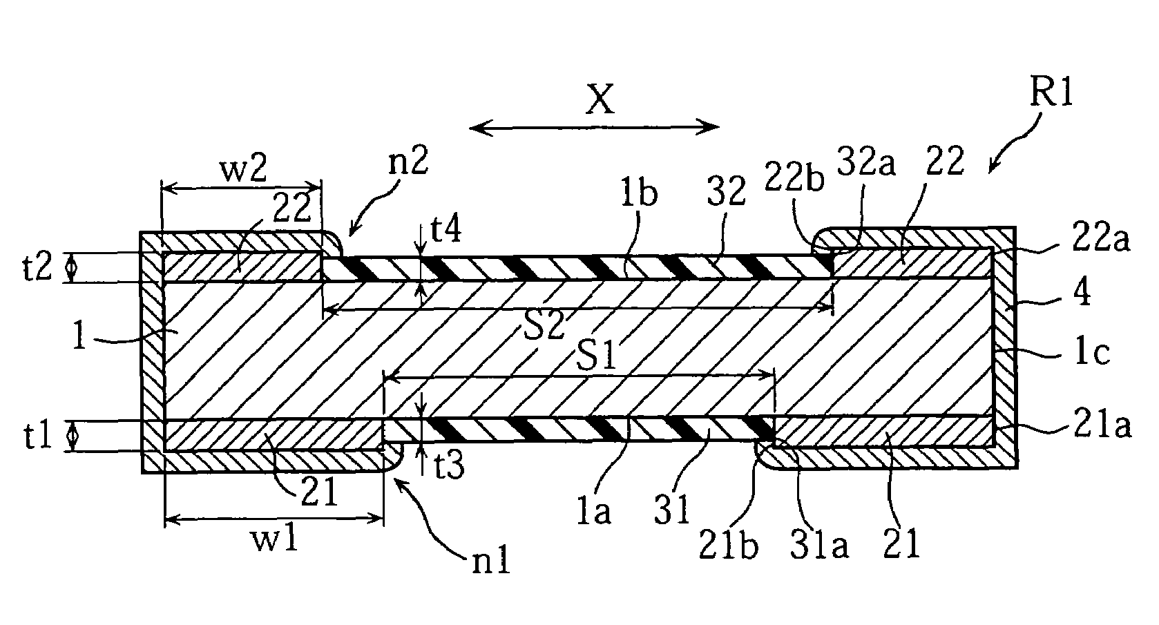
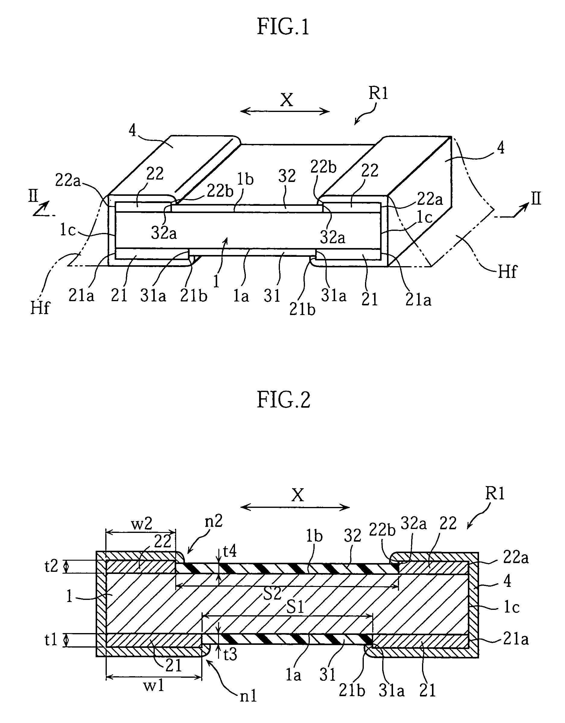
[0035]FIGS. 1 to 2 illustrate a chip resistor according to the present invention. The illustrated chip resistor R1 includes a resistor element 1, a pair of main electrodes 21, a pair of auxiliary electrodes 22, first and second insulating layers 31, 32, and a pair of solder layers 4.

[0036]The resistor element 1 is a rectangular chip made of a metal and has a constant thickness. Examples of material for forming the resistor element 1 include Ni—Cu alloy or Cu—Mn alloy, though not limited to these. The material of the resistor element 1 may be selected from materials having a resistivity suited to provide the chip resistor R1 with an intended resistance.

[0037]The pair of main electrodes 21 and the pair of auxiliary electrodes are made of a same material such as copper, for example. Each of the main electrodes 21 is formed on a lower surface 1a of the resistor element 1,...


PUM


Abstract

A chip resistor (R1) includes a resistor element (1) having a first surface (1a) and a second surface (1b) opposite to the first surface. Two main electrodes (21), spaced from each other, are provided on the first surface (1a), while two auxiliary electrodes (22), spaced from each other, are provided on the second surface (1b). The auxiliary electrodes face the main electrodes (21) via the resistor element (1). The main electrodes (21) and the auxiliary electrodes (22) are made of the same material.

Description

TECHNICAL FIELD[0001]The present invention relates to a chip resistor and a method of making the same.BACKGROUND ART[0002]FIGS. 10 and 11 illustrate a conventional chip resistor. The chip resistor 1A shown in FIG. 10 is disclosed in JP-A-2002-57009, and the chip resistor 2A shown in FIG. 11 is disclosed in JP-A-2002-57010.[0003]As shown in FIG. 10, the chip resistor 1A includes a metal resistor element 100 and a pair of copper electrodes 110. The electrodes 110 are fixed to a lower surface 100a of the resistor element 100 and spaced from each other in the direction X in the figure. Each of the electrodes 110 includes a lower surface provided with a solder layer 130.[0004]The chip resistor 1A is surface-mounted on e.g. printed circuit board, using solder. It is desirable that melted solder uniformly contacts with the entire lower surface of each of the electrode 110. However, the melted solder may contact only with an inner surface 111 and its vicinity of the electrode 110. The melte...

Claims


Application Information

Patent Timeline
Patent Type & Authority Patents(United States)
IPC IPC(8): H01L23/62H01C1/028H01C1/03H01C3/00H01C1/14H01C7/00H01C17/00
CPCH01C1/14H01C7/003H01C17/006H01C3/00
Inventor TSUKADA, TORAYUKI
Owner ROHM CO LTD
Why Eureka
Try Eureka