High speed circuit assembly with integral terminal and mating bias loading electrical connector assembly

a technology of bias loading and circuit assembly, which is applied in the direction of electrical apparatus construction details, coupling device connections, conductive pattern formation, etc., can solve the problems of carbon contamination, high cost of flexible circuits compared to some rigid pcb products, and limited layer count or feature registration of flexible circuits. , to achieve the effect of attractive manufacturing cost and high density

Active Publication Date: 2015-05-21
HSIO TECH
View PDF7 Cites 36 Cited by
  • Summary
  • Abstract
  • Description
  • Claims
  • Application Information

AI Technical Summary

Benefits of technology

[0012]The present disclosure relates to a high density electrical interconnect between at least two components, such as a high density circuit to a low density PCB. By combining methods used in the PCB fabrication and semiconductor packaging industries, the present disclosure enables fine line high density circuit structures with attractive cost of manufacture.
[0013]The present disclosure adds a bulk conductive material to create very small low resistance terminals to increase density and reduce line and feature pitch of the circuits as well as a host of electrical enhancements that provide an electrical circuit that may prove to be superior to the traditional methods. The terminal can be created with various features, including undercuts, that cannot be formed using dry film technology.
[0018]The vias and associated circuit geometry can be imaged in the liquid dielectric in a variety of shapes and sizes, depending on the terminal structure on the circuit members. The contact members and vias can be positioned at a variety of locations, heights, or spacing to match the parameters of existing connections making it easy to replace an existing circuit without changing hardware or the PCB. The present disclosure permits the creation of blind or buried conductive structures on very tight pitch of about 25 microns or below without the use of laser ablation.
[0019]Traditional PCB and flex circuit fabrication methods take sheets of material and stack them up, laminate, and / or drill. The materials in each layer are limited to the materials in a particular sheet. The present disclosure employs a liquid dielectric that is image, permitting a wide variety of materials to be applied on a single layer with a registration relative to the features of the previous layer. Selective addition of conductive, non-conductive, or semi-conductive materials at precise locations to create a desired effect has the major advantages in tuning impedance or adding electrical function on a given layer. Tuning performance on a layer by layer basis relative to the previous layer greatly enhances electrical performance.

Problems solved by technology

In general, flexible circuits are expensive compared to some rigid PCB products.
Flexible circuits also have some limitations regarding layer count or feature registration, and are therefore generally only used for small or elongated applications.
Rigid PCBs and package substrates experience challenges as the feature sizes and line spacing are reduced to achieve further miniaturization and increased circuit density.
As density increases, however, laser processed via structures can experience significant taper, carbon contamination, layer-to-layer shorting during the plating process due to registration issues, and high resistance interconnections that may be prone to result in reliability issues.
The challenge of making fine line PCBs often relates to the difficulty in creating very small or blind and buried vias.
In both cases, the package substrate and the larger format circuit board build up are very expensive compared to traditional low density laminate technology, and suffer from several limitations inherent to the process.
For example, in the case where a low density laminate base is used as the starting point for subsequent high density layers are built up, the cost increases dramatically since the entire surface of the lower density base board must be processed with the build up process across the entire area, not just in the areas where the high density is required.
Another limitation is the reliability of the via structures joining one circuit layer to another, which tend to be a barrel plated structures with the side walls of the via plated and in many cases must be filled with a via fill material to eliminate an air pocket which may separate during solder reflow temperatures.

Method used


Image

  • High speed circuit assembly with integral terminal and mating bias loading electrical connector assembly
  • High speed circuit assembly with integral terminal and mating bias loading electrical connector assembly
  • High speed circuit assembly with integral terminal and mating bias loading electrical connector assembly

Examples


Embodiment Construction

[0041]A high density circuit structure according to the present disclosure may permit fine contact-to-contact spacing (pitch) on the order of less than 1.0 mm pitch, and more preferably a pitch of less than about 0.7 millimeter, and most preferably a pitch of less than about 0.4 millimeter. Such fine pitch high density circuit structures are especially useful for communications, wireless, and memory devices.

[0042]The present high density circuit structure can be configured as a low cost, high signal performance electrical interconnect assembly, which has a low profile that is particularly useful for desktop and mobile PC applications. IC devices can be installed and uninstalled without the need to reflow solder. The solder-free electrical connection of the IC devices is environmentally friendly. In another embodiment, the high density circuit structure can also be a portion of a socket or semiconductor package.

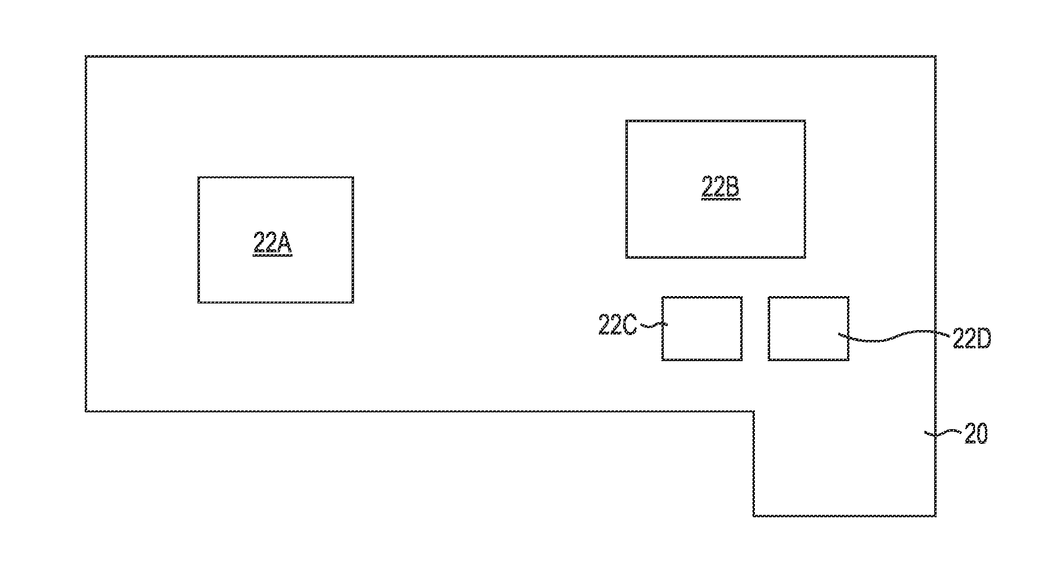
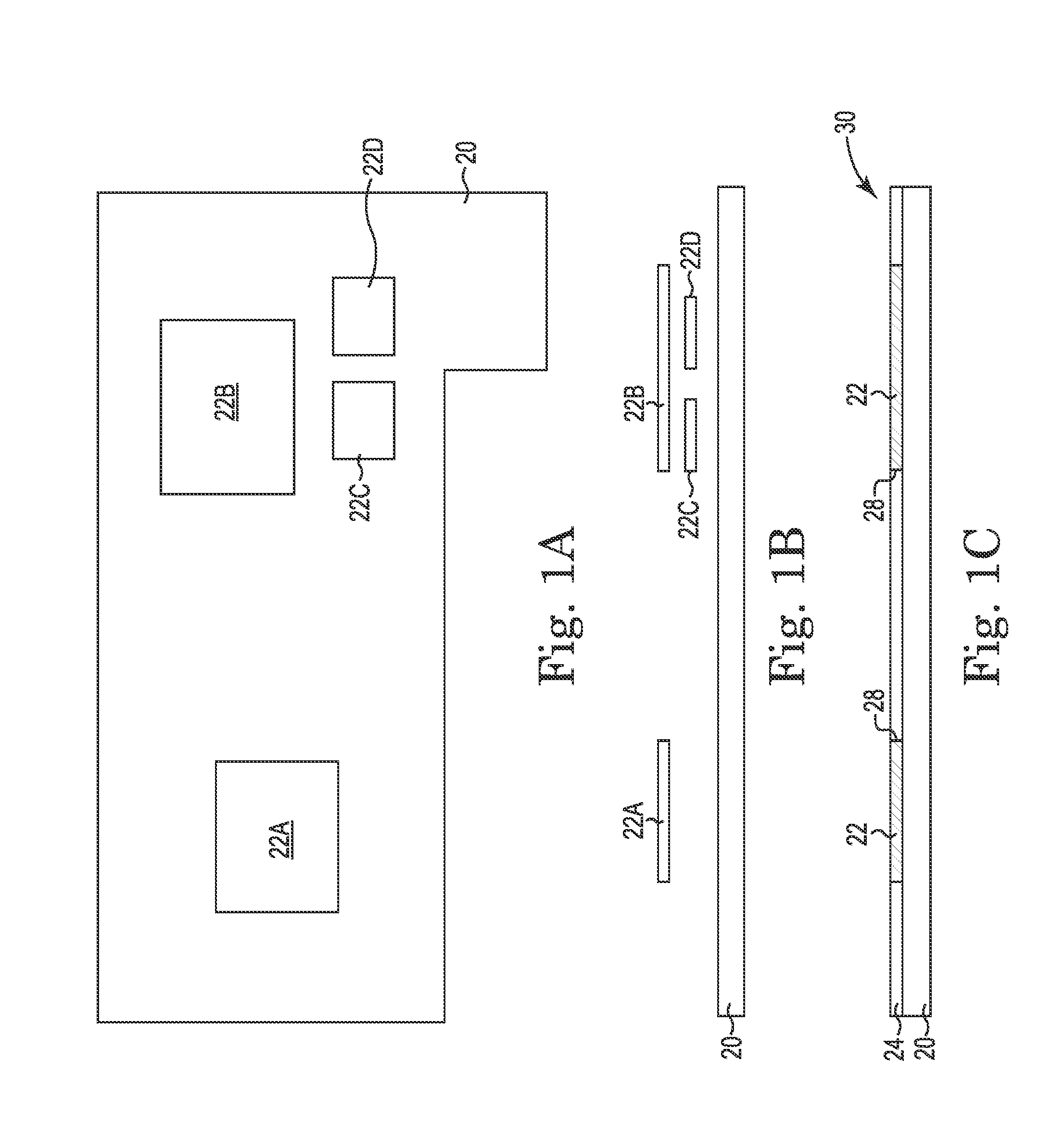
[0043]FIGS. 1A and 1B schematically illustrate the merger of a lower dens...


PUM

PropertyMeasurementUnit
aspect ratioaaaaaaaaaa

Abstract

A method of making an array of integral terminals on a circuit assembly. The method includes the steps of depositing at least a first liquid dielectric layer on the first surface of a first circuit member, imaged to include a plurality of first recesses corresponding to the array of integral terminals. The selected surfaces of the first recesses are processed to accept electro-less conductive plating deposition. Electro-lessly plating is applied to the selected surfaces of the first recesses to create a plurality of first conductive structures electrically coupled to, and extending generally perpendicular to, the first circuitry layer. Electro-plating is applied to the electro-less plating to substantially first recesses with a conductive material. The steps of depositing, processing, electro-less plating, and electro-plating are repeated to form the integral terminals of a desired shape. The dielectric layers are removed to expose the terminals.

Description

CROSS-REFERENCE TO RELATED APPLICATIONS[0001]This application claims the benefit of U.S. Provisional Application No. 61 / 669,893, filed Jul. 10, 2012, the disclosure of which is hereby incorporated by reference.TECHNICAL FIELD[0002]The present disclosure relates to a high density electrical interconnect between at least two components in an electronic system using a unique circuit structure fabrication technique that leverages processes used in the printed circuit and semiconductor packaging industries.BACKGROUND OF THE INVENTION[0003]Traditional printed circuits are often constructed in what is commonly called rigid or flexible formats. The rigid versions are used in nearly every electronic system, where the printed circuit board (PCB) is essentially a laminate of materials and circuits that when built is relatively stiff or rigid and cannot be bent significantly without damage.[0004]Flexible circuits have become very popular in many applications where the ability to bend the circui...

Claims


Application Information

Patent Timeline
Patent Type & Authority Applications(United States)
IPC IPC(8): H01R12/77H01R12/82H01R12/79
CPCH01R12/772H01R12/82H01R12/79H01R12/778H05K1/141H05K3/326H05K3/4092H05K7/1076H05K2201/0397H05K2201/10378H05K2203/041H01L24/16H01L24/48H01L2224/16225H01L2224/48091H01L2924/00014H01L2924/12042H01L2924/15311H01R12/73H05K1/092H05K1/111H05K1/182H05K3/0094H05K3/363H05K3/365H05K3/4007H05K3/4015H05K3/425H05K3/4694H05K2201/048H05K2201/09381H05K2201/09545H05K2201/09563H05K2201/09854H05K2201/10386H05K2201/2072H05K2201/209H05K2203/1476H01L2224/45144Y10T29/49165H01L2224/45099H01L2924/00H01R13/2485H01R12/00H01R31/06H05K3/10H05K3/1291H01R13/2457
Inventor RATHBURN, JAMES
Owner HSIO TECH
Why Eureka
Try Eureka