High performance electrical circuit structure

a high-performance, electrical interconnection technology, applied in the association of printed circuit non-printed electric components, semiconductor/solid-state device details, dielectric characteristics, etc., can solve the problems of carbon contamination, laser processing via structure can experience significant taper, and flexible circuits are expensive compared to some rigid pcb products, etc., to achieve attractive manufacturing cost and high density

Active Publication Date: 2016-01-05
LCP MEDICAL TECH LLC
View PDF433 Cites 7 Cited by
  • Summary
  • Abstract
  • Description
  • Claims
  • Application Information

AI Technical Summary

Benefits of technology

[0013]The present disclosure is directed to a high performance electrical interconnect that will enable next generation electrical performance. The present disclosure merges the long-term performance advantages of traditional PCB and semiconductor packaging with the flexibility of additive printing technology. By combining methods used in the PCB fabrication and semiconductor packaging industries, the present disclosure enables fine line high density circuit structures with attractive cost of manufacture.
[0014]The present disclosure includes adding a bulk material to create the vias and other circuit geometry to supplement or replace the traditional circuit production techniques. This approach enables the production of very small low resistance vias to increase density and reduce line and feature pitch of the circuits as well as a host of electrical enhancements that provide an electrical interconnect that may prove to be superior to the traditional methods. In basic terms, the structure leverages methods used in the semiconductor packaging industry such as stud bumping, ball bonding, flip chip, or pillar termination or discrete particles or spheres of copper, solder or precious metal to act as the via connecting layers within the circuit stack.
[0015]The present high performance electrical interconnect can be treated as a system of its own by incorporating electrical devices or other passive and active function, such as for example, ground planes, power planes, electrical connections to other circuit members, dielectric layers, conductive traces, transistors, capacitors, resistors, RF antennae, shielding, filters, signal or power altering and enhancing devices, memory devices, embedded IC, and the like. In some embodiments, the electrical devices can be formed using printing technology, adding intelligence to the interconnect assembly.

Problems solved by technology

In general, flexible circuits are expensive compared to some rigid PCB products.
Flexible circuits also have some limitations regarding layer count or feature registration, and are therefore generally only used for small or elongated applications.
Rigid PCBs and package substrates experience challenges as the feature sizes and line spacing are reduced to achieve further miniaturization and increased circuit density.
As density increases, however, laser processed via structures can experience significant taper, carbon contamination, layer-to-layer shorting during the plating process due to registration issues, and high resistance interconnections that may be prone to result in reliability issues.
The challenge of making fine line PCBs often relates to the difficulty in creating very small or blind and buried vias.

Method used


Image

  • High performance electrical circuit structure
  • High performance electrical circuit structure
  • High performance electrical circuit structure

Examples


Embodiment Construction

[0052]A high performance electrical interconnect according to the present disclosure may permit fine contact-to-contact spacing (pitch) on the order of less than 1.0 mm pitch, and more preferably a pitch of less than about 0.7 millimeter, and most preferably a pitch of less than about 0.4 millimeter. Such fine pitch high performance electrical interconnects are especially useful for communications, wireless, and memory devices.

[0053]The present high performance electrical interconnect can be configured as a low cost, high signal performance interconnect assembly, which has a low profile that is particularly useful for desktop and mobile PC applications. IC devices can be installed and uninstalled without the need to reflow solder. The solder-free electrical connection of the IC devices is environmentally friendly.

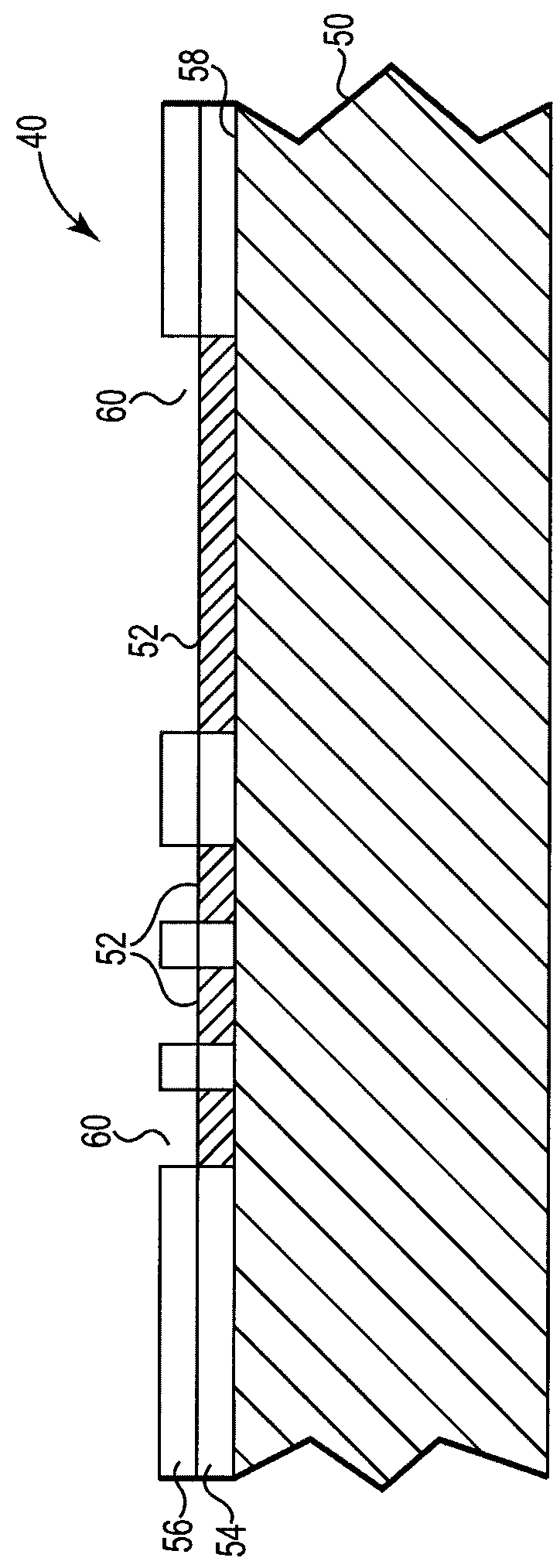
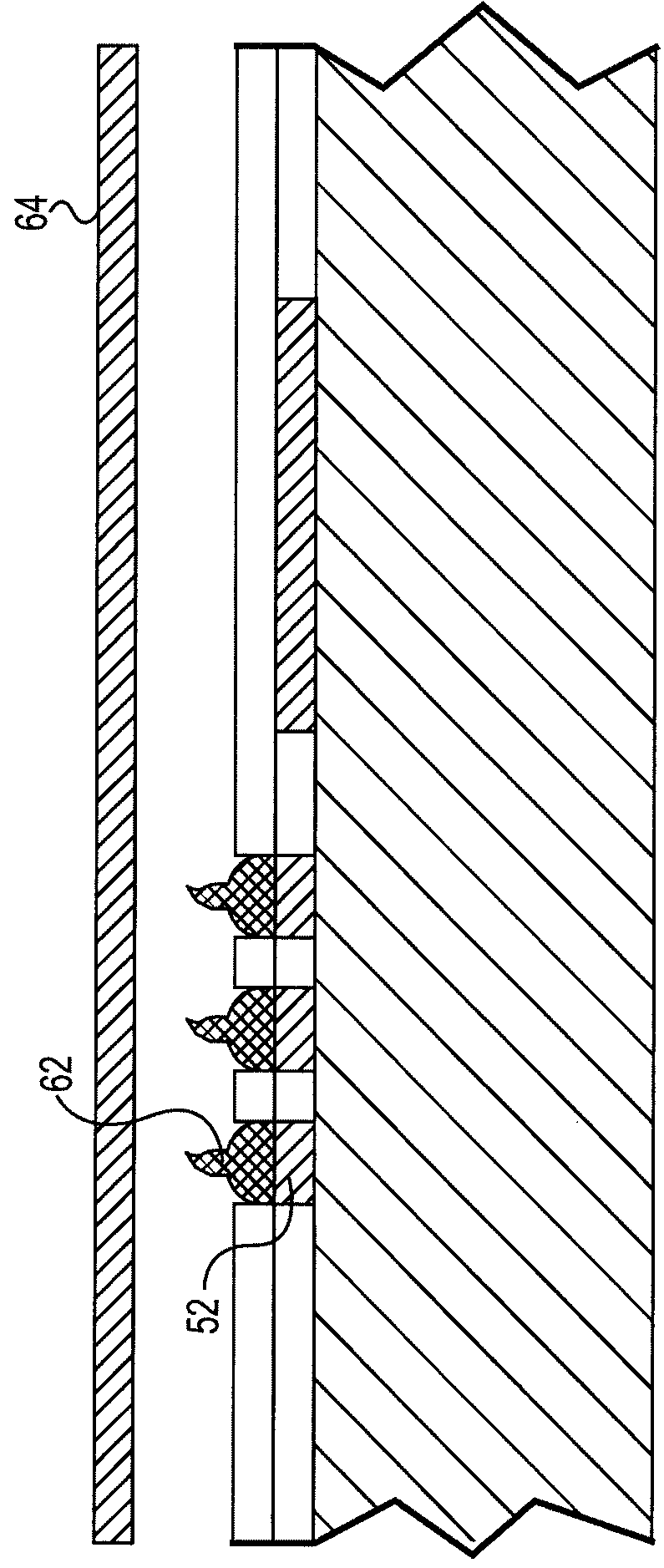
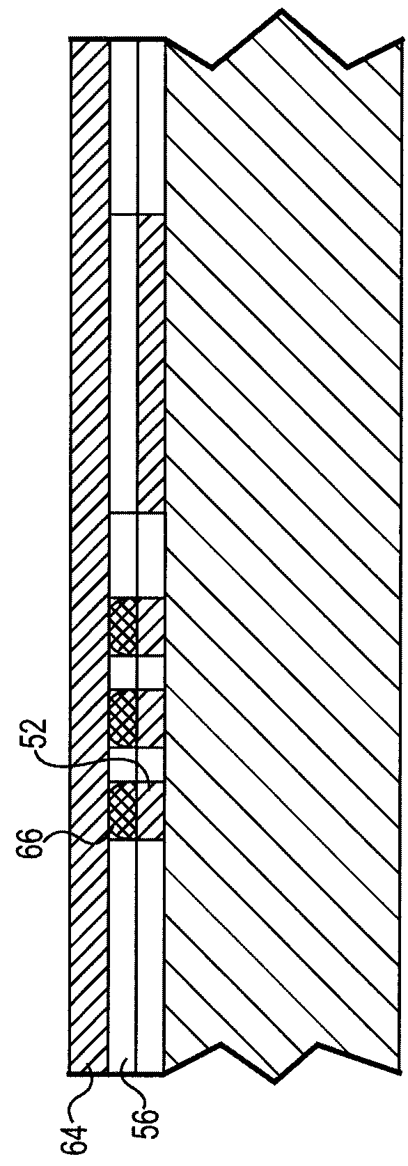
[0054]FIG. 1 is a side cross-sectional view of a method of making an electrical interconnect 40 using additive processes in accordance with an embodiment of the present dis...


PUM

PropertyMeasurementUnit
conductiveaaaaaaaaaa
optical qualityaaaaaaaaaa
flexibleaaaaaaaaaa

Abstract

A high performance electrical interconnect adapted to provide an interface between terminals on first and second circuit members. The electrical interconnect includes a first circuitry layer with a first surface and a second surface having a plurality of contact pads adapted to electrically coupled with the terminals on the first circuit member. At least one dielectric layer is printed on the first surface of the first circuitry layer. The dielectric layer includes a plurality recesses. A conductive material is deposited in at least a portion of the recesses to create circuit geometry electrically coupled with the first circuitry layer. A second circuitry layer includes a first surface a plurality of contact pads adapted to electrically couple with the terminals on the second circuit member and a second surface attached to the dielectric layers. The circuit geometry electrically couples the first circuitry layer to the second circuitry layer.

Description

CROSS-REFERENCE TO RELATED APPLICATIONS[0001]This application claims the benefit of a national stage application under 35 U.S.C. §371 of International Application No. PCT / US2011 / 056664, titled HIGH PERFORMANCE ELECTRICAL CIRCUIT STRUCTURE, filed Oct. 18, 2011, which claims priority to U.S. Provisional Application No. 61 / 406,286, filed Oct. 25, 2010, all of which are hereby incorporated by reference in their entireties.[0002]This application is a continuation-in-part of U.S. patent application Ser. No. 13 / 318,171, titled COMPLIANT PRINTED CIRCUIT PERIPHERAL LEAD SEMICONDUCTOR TEST SOCKET, filed Oct. 31, 2011, which is a national stage application under 35 U.S.C. §371 of International Application No. PCT / US2010 / 036397, titled COMPLIANT PRINTED CIRCUIT PERIPHERAL LEAD SEMICONDUCTOR TEST SOCKET, filed May 27, 2010, which claims priority to U.S. Provisional Application No. 61 / 183,378, filed Jun. 2, 2009, both of which are hereby incorporated by reference in their entireties.[0003]This ap...

Claims


Application Information

Patent Timeline
Patent Type & Authority Patents(United States)
IPC IPC(8): H05K1/00H05K3/32H05K3/40H01L23/538H05K1/18H05K3/46H05K3/30H05K1/11H05K1/16H05K3/12H01L23/498H05K1/02
CPCH05K3/4664H05K1/18H01L23/5383H05K1/111H05K1/115H05K1/16H05K3/1291H05K3/30H05K3/325H05K3/4007H01L23/49811H01L2224/16H01L2924/09701H01L2924/12044H05K1/0274H05K2201/0133Y10T29/49155
Inventor RATHBURN, JAMES
Owner LCP MEDICAL TECH LLC
Why Eureka
Try Eureka