Finned field-effect transistor (FET) and forming method thereof

A fin field effect and transistor technology, which is applied to semiconductor devices, semiconductor/solid-state device manufacturing, electrical components, etc., can solve the problems of serious self-heating effect of fin field effect transistors, and achieves serious self-heating effect. The effect of increased area and improved reliability

Active Publication Date: 2015-02-11
SEMICON MFG INT (SHANGHAI) CORP
View PDF2 Cites 5 Cited by
  • Summary
  • Abstract
  • Description
  • Claims
  • Application Information

AI Technical Summary

Problems solved by technology

[0006] The problem solved by the present invention is to provide a fin field effect transistor and its forming method to solve the serious problem of the self-heating effect of the fin field effect transistor and improve the reliability of the fin field effect transistor

Method used


Image

  • Finned field-effect transistor (FET) and forming method thereof
  • Finned field-effect transistor (FET) and forming method thereof
  • Finned field-effect transistor (FET) and forming method thereof

Examples


Embodiment Construction

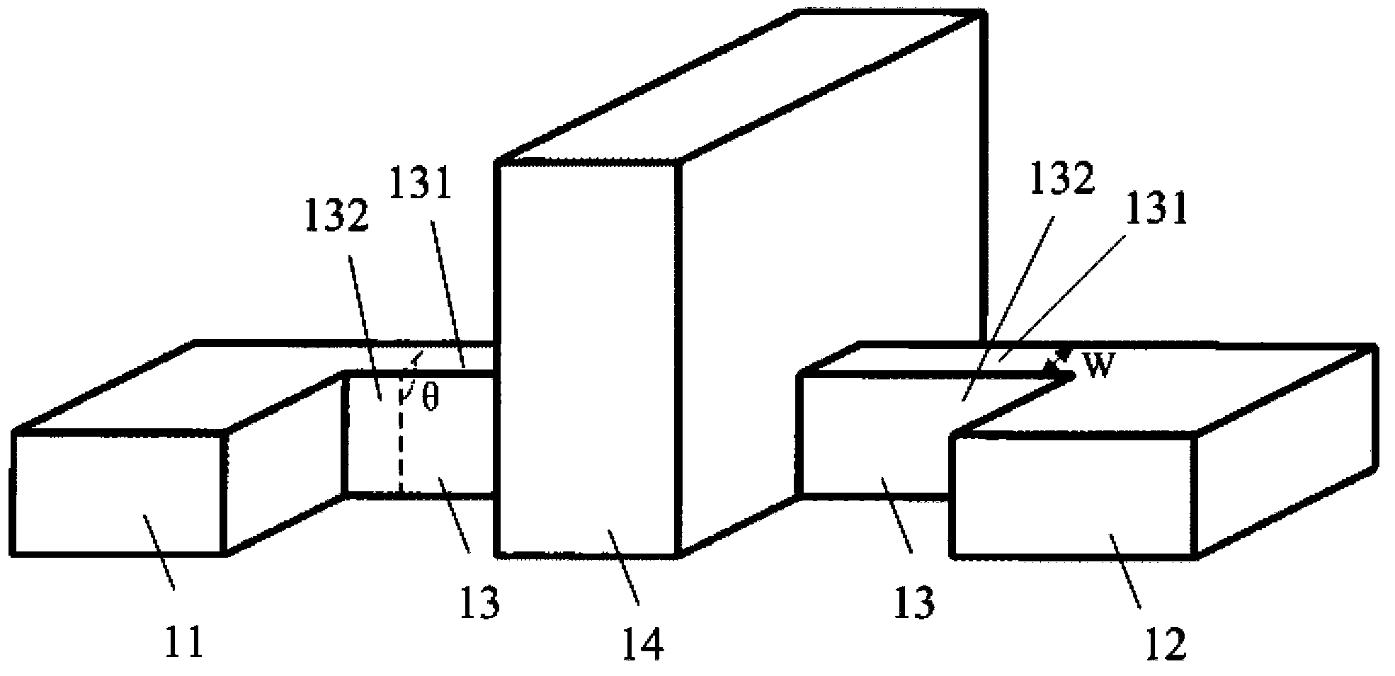
[0040] As mentioned in the background art, because the upper surface of the existing fin field effect transistor is flat, and there is a vertical corner between the upper surface and the side surface, on the one hand, the overall width of the fin structure of the fin field effect transistor is large, It is difficult to dissipate heat. On the other hand, the parasitic resistance of the channel area formed inside the fin structure is large, which leads to serious heating effects when the current passes through the channel area. Two reasons lead to the self-heating of the existing fin field effect transistor. The effect is serious, so that the fin field effect transistor has serious reliability problems.

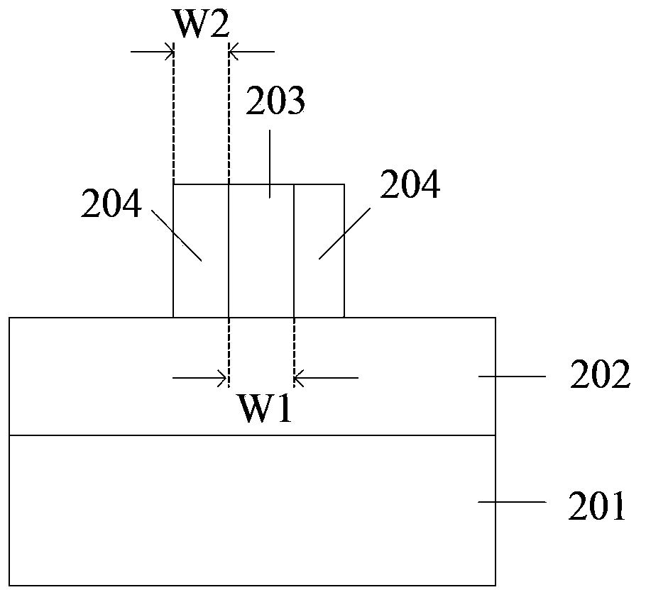
[0041] To this end, the present invention provides a method for forming a Fin Field Effect Transistor, in which a semiconductor-on-insulator semiconductor layer is patterned to form a fin structure, and then a mask layer is formed in the middle of the upper surface of the fin st...


PUM


Abstract

The invention provides a finned field-effect transistor (FET) and a forming method thereof. The forming method of the finned FET comprises the steps: providing an on-insulator semiconductor substrate, wherein the on-insulator semiconductor substrate comprises a semiconductor layer; patterning the semiconductor layer until fin part structures, of which the upper surfaces are level, are formed; forming mask layers at the middle parts of the upper surfaces of the fin part structures; carrying out first-time anisotropic etching on the fin part structures in a manner of taking the mask layers as masks until the exposed upper surfaces of the fin part structures are etched into curved surfaces; removing the mask layers. The forming method is simple in process and low in process cost, and the formed finned FET is free from the problem of serious self-heating effect.

Description

technical field [0001] The invention relates to the technical field of semiconductors, in particular to a fin field effect transistor and a forming method thereof. Background technique [0002] As the feature size of semiconductor devices enters the nanometer scale, fin field effect transistors (FinFETs) are introduced to optimize the electrical characteristics of the devices. [0003] However, the existing fin field effect transistor has relatively serious self-heating effect. The self-heating effect of the fin field effect transistor will reduce the on-state current of the transistor, increase the leakage current, reduce the switching ratio of the transistor, cause the degradation of the performance of the transistor, the circuit and even the system, and cause serious reliability problems. [0004] Please refer to figure 1 , the existing fin field effect transistor includes a source 11 in silicon-on-insulator (SOI, not shown), a drain 12, a fin structure 13 and a gate 14...

Claims


Application Information

Patent Timeline
Patent Type & Authority Applications(China)
IPC IPC(8): H01L21/336H01L21/308H01L29/78H01L29/06
CPCH01L21/3065H01L29/06H01L29/66795H01L29/785
Inventor 张海洋张城龙
Owner SEMICON MFG INT (SHANGHAI) CORP
Why Eureka
Try Eureka