
Display apparatus

A technology of display device and display area, which is applied to static indicators, instruments, semiconductor devices, etc., and can solve problems such as deterioration of sub-pixel image quality.

Active Publication Date: 2015-02-11
SAMSUNG DISPLAY CO LTD
View PDF6 Cites 14 Cited by
  • Summary
  • Abstract
  • Description
  • Claims
  • Application Information

AI Technical Summary

Problems solved by technology

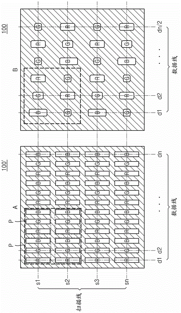
[0009] For the 2G / 1B / 1R five-tile matrix structure described above, it is difficult to use it for high resolution greater than 440 sub-pixels per inch (ppi), and during actual image reproduction each repeated group Reduced number of sub-pixels can degrade image quality

Method used


Image

  • Display apparatus
  • Display apparatus
  • Display apparatus

Examples


Embodiment Construction

[0042]Reference will now be made in detail to embodiments, examples of which are illustrated in the accompanying drawings, wherein like reference numerals refer to like elements throughout. In this regard, the present embodiments may have different forms and should not be construed as limited to the embodiments set forth herein. Accordingly, the embodiments are merely described below, by referring to the figures, to illustrate aspects of the present teachings. The term "and / or", when used in the present invention, includes any and all combinations of one or more of the associated listed items. Expressions such as "at least one of" when preceding a series of elements modify the entire series of elements and do not modify individual elements of the series.

[0043] The embodiments set forth herein are exemplary only, and various modifications can be made in the embodiments without departing from the spirit and scope of the present teachings. For example, it will be understood ...


PUM


Abstract

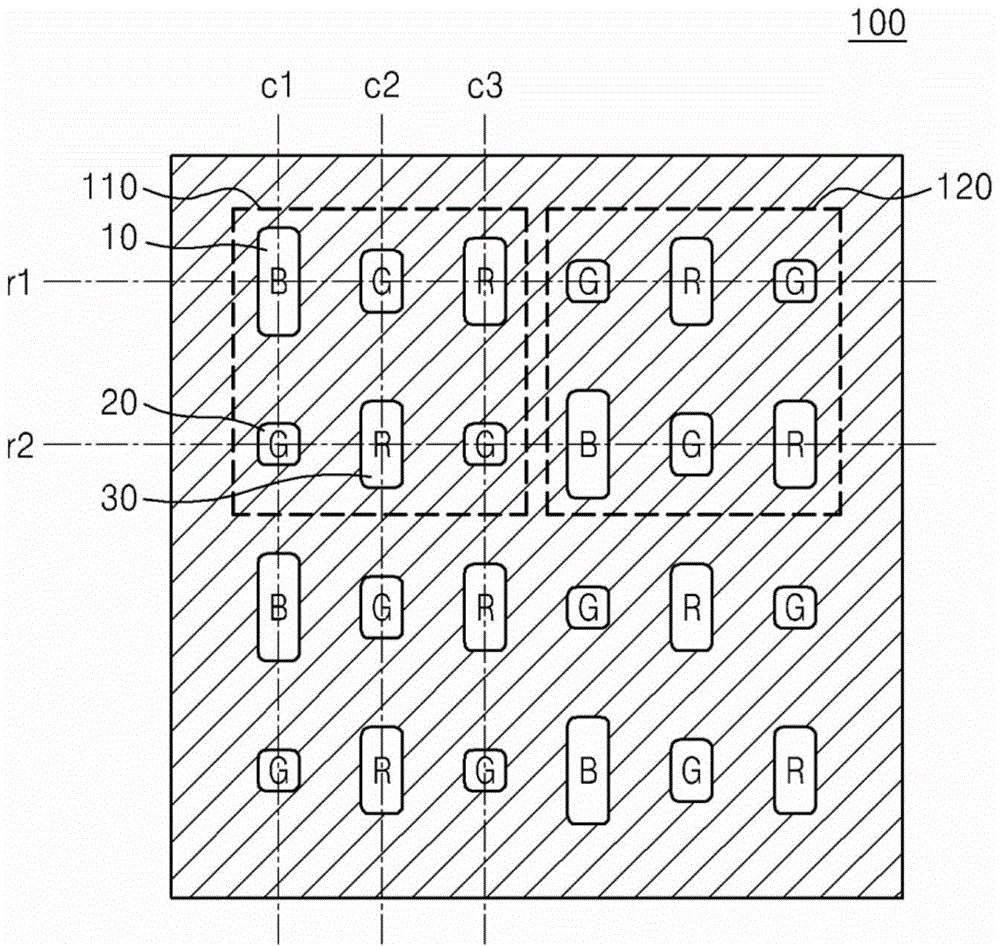
A pixel array structure for populating the display area of a display device (100, 200, 300, 400) includes a repeated first pixel group (110) that consists of one or more first colored subpixels (10), three or more second colored subpixels (20) and two or more third colored subpixels (30). The respective numbers of the first colored subpixels, the second colored subpixels, and the third colored subpixels that are provided within the first pixel group are preferably in a respective ratio of 1:3:2. In one embodiment, an input RGB image is remapped to have luminance values corresponding to Cyan-Magenta-Yellow coordinates and the latter are used in combination with subpixel rendering (SPR) to drive the colored subpixels of the pixel array structure.

Description

[0001] related application [0002] This application claims the benefit of Korean Patent Application No. 10-2013-0088177 filed with the Korean Intellectual Property Office on Jul. 25, 2013, the entire disclosure of which is incorporated herein by reference. technical field [0003] The present disclosure relates to a pixel array structure and a display device including the same, and more particularly, the present disclosure relates to providing user perception with high image resolution while allowing increased mass production rates and longer devices lifetime of the pixel array structure. Background technique [0004] With the recent rapid development of semiconductor technology, the typical screen size of a flat panel display device has gradually increased, however it is still expected that the weight of the device should be reduced. Furthermore, the demand for flat panel display devices having such excellent characteristics has grown explosively. [0005] Examples of su...

Claims


Application Information

Patent Timeline
Patent Type & Authority Applications(China)
IPC IPC(8): H01L27/32
CPCG09G2300/0452G09G3/2074G09G3/3225G09G3/2092G09G3/2003G09G2340/0457H10K59/30H10K59/122H10K50/84
Inventor 金建植
Owner SAMSUNG DISPLAY CO LTD
Learn More