
Optical Modules and Optical Transmitters

An optical module and optical waveguide technology, applied in optics, instruments, nonlinear optics, etc., can solve the problems of increasing the size of the module and increasing the size

Active Publication Date: 2018-01-23
FUJITSU OPTICAL COMPONENTS LTD
View PDF12 Cites 0 Cited by
  • Summary
  • Abstract
  • Description
  • Claims
  • Application Information

AI Technical Summary

Problems solved by technology

This causes the problem that the size of the relay substrate (e.g. along the length of the parallel waveguides of the Mach-Zehnder modulator unit) increases and the size of the module housing the Mach-Zehnder modulator unit also increases

Method used


Image

  • Optical Modules and Optical Transmitters
  • Optical Modules and Optical Transmitters
  • Optical Modules and Optical Transmitters

Examples


Embodiment Construction

[0023] Embodiments of the optical module and the optical transmitter will be described in detail with reference to the accompanying drawings.

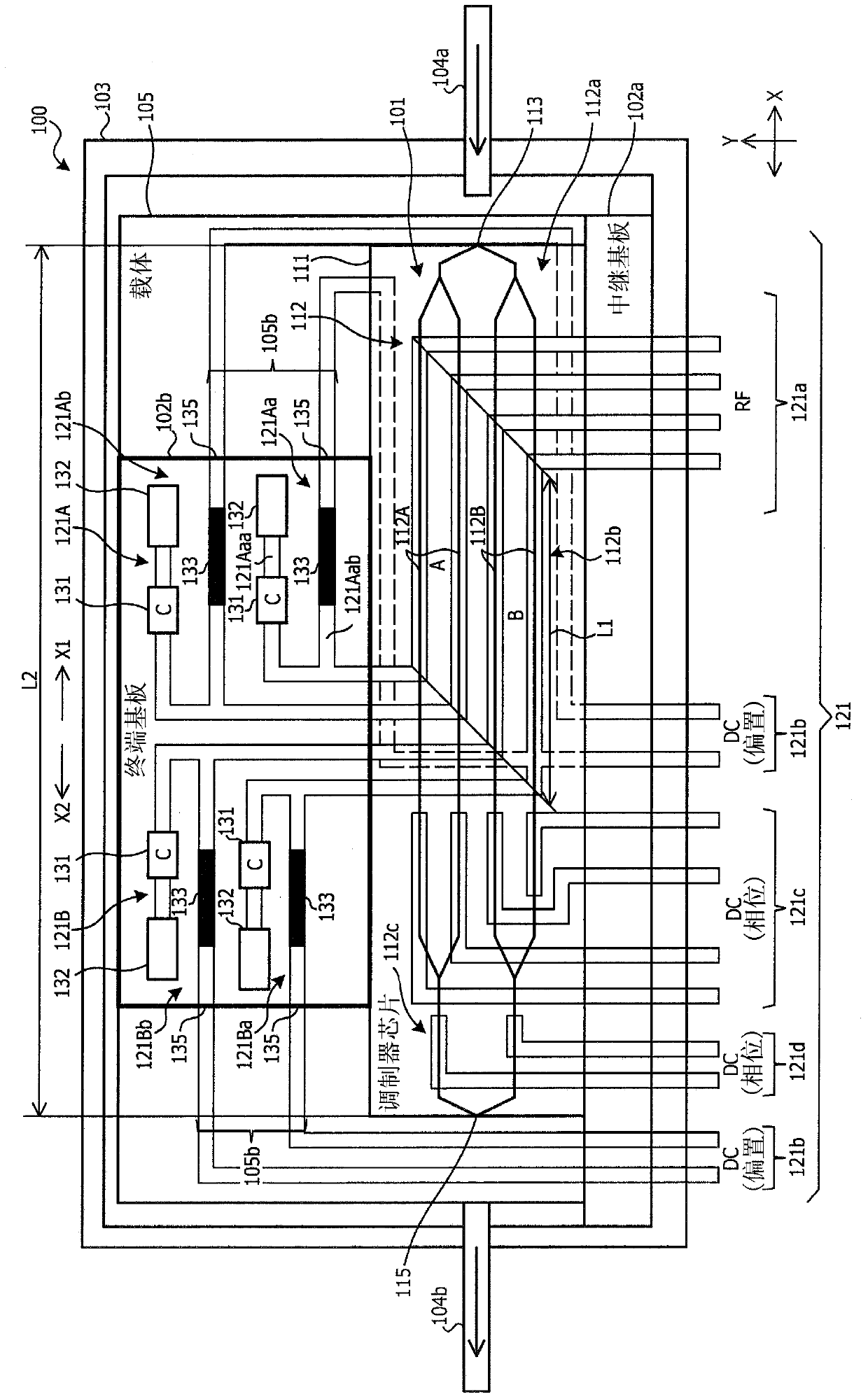
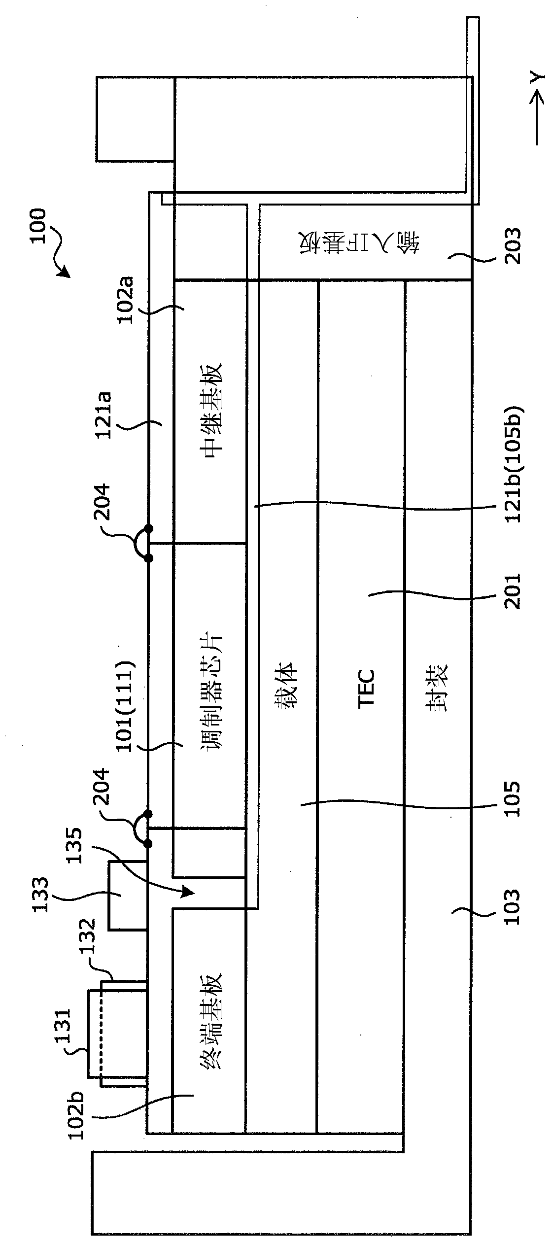
[0024] figure 1 is a top view of the optical module according to the first embodiment, figure 2 is a side sectional view of the optical module according to the first embodiment. This optical module 100 is a construction example of a QPSK optical modulator, including a Mach-Zehnder modulator unit (modulator chip) 101, an electrode substrate 102, and a housing (packaging) for accommodating the Mach-Zehnder modulator unit 101 and the electrode substrate 102 103 , input / output optical fiber 104 ( 104 a , 104 b ), carrier (substrate) 105 . A plurality of terminals (RF terminals and DC terminals, which will be described later) are formed on the electrode substrate 102 .

[0025] On the carrier 105 in the housing 103 the waveguide substrate 111 of the Mach-Zehnder modulator unit (modulator chip) 101 is arranged. On the carrier 105 , the ...


PUM


Abstract

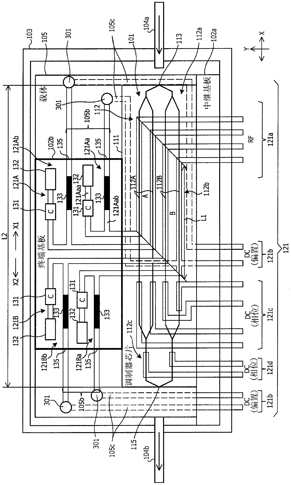
Optical modules and optical transmitters. An optical module comprising: a waveguide substrate, comprising a light waveguide and multiple electrodes that apply an electrical signal to the optical waveguide; Relay substrate, arranged adjacent to the waveguide substrate; The terminal substrate, adjacent to the waveguide substrate and arranged oppositely from the relay substrate across the waveguide substrate; Carrier substrate, the waveguide substrate, the relay substrate, the terminal substrate is mounted on the carrier substrate. The plurality of electrodes having a first interconnect unit from the relay substrate via the waveguide substrate to the terminal substrate and a plurality of second interconnect units branching from the first interconnecting unit and on the terminal substrate. In the second interconnect unit, the first interconnect branch comprises a capacitor and a termination resistor; The second interconnect branch is connected via a bias resistor to the interconnect portion of the carrier substrate, passing under the waveguide substrate, to the DC electrode for bias adjustment on the relay substrate.

Description

technical field [0001] Embodiments discussed herein relate to optical modules and optical transmitters used in optical transmission. Background technique [0002] For example using electro-optic crystal substrates such as LiNbO 3 (LN) substrate and LiTaO 2 substrates) or semiconductor substrates (such as GaAs substrates and InP substrates) are considered to be optical modules. This optical waveguide device is formed by forming a metal film made of titanium (Ti) on a part of a substrate and thermally diffusing the film, or by performing proton exchange in benzoic acid after a patterning process. Electrodes are then formed near the optical waveguide to construct an optical module, such as an optical modulator. [0003] When driving such an optical modulator at high speed, it is assumed that the terminal of the signal electrode is connected to the terminal of the ground electrode via a resistor to form a traveling wave electrode, and a high-speed microwave signal (electrical...

Claims


Application Information

Patent Timeline
Patent Type & Authority Patents(China)
IPC IPC(8): H04B10/556
CPCG02F1/2255G02F2201/16H04B10/501H04B10/532G02F1/212G02F1/225
Inventor 杉山昌树佐佐木诚美田中刚人
Owner FUJITSU OPTICAL COMPONENTS LTD
Learn More