A dual frequency metamaterial absorber
A technology of metamaterials and absorbers, applied to electrical components, antennas, etc., can solve problems such as poor stability, and achieve the effect of wide incident angle and high absorption rate
- Summary
- Abstract
- Description
- Claims
- Application Information
AI Technical Summary
Problems solved by technology
Method used
Image
Examples
Embodiment Construction
[0017] The present invention will be further described in detail below in conjunction with the accompanying drawings and specific embodiments.
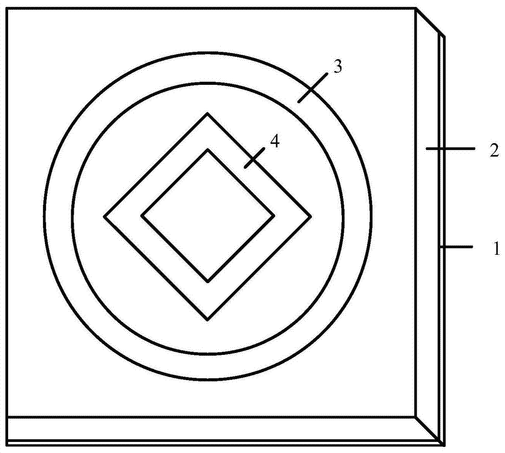
[0018] combine figure 1 , Fig. 2 (A) and Fig. 2 (B), the present invention is made up of bottom metal thin film 1, middle loss dielectric layer 2 and top layer metal thin film arranged successively from bottom to top, bottom metal thin film 1, middle loss dielectric layer 2 and the top metal film are attached to each other, that is, the bottom metal film 1 and the top metal film of the present invention are respectively attached to both sides of the middle lossy dielectric layer 2, and the bottom metal film 1 is an all-metal film without a hollow structure , the top metal film consists of a metal ring 3 and a metal square ring 4 located in the metal ring 3, the center of the metal ring 3 and the center of the metal square ring 4 and the center of the middle lossy dielectric layer 2 and the bottom metal film 1 The center is on a strai...
PUM
| Property | Measurement | Unit |
|---|---|---|
| size | aaaaa | aaaaa |
Abstract
Description
Claims
Application Information


